Liquid metal interconnects

a liquid metal interconnect and metal alloy technology, applied in the field of integrated circuit devices, can solve the problems of enormous performance demands on techniques and materials, ever-smaller integrated circuits,

Active Publication Date: 2013-01-03
INTEL CORP
View PDF21 Cites 13 Cited by
  • Summary
  • Abstract
  • Description
  • Claims
  • Application Information

AI Technical Summary

Problems solved by technology

The push for ever-smaller integrated circuits (IC) places enormous performance demands on the techniques and materials used to construct and test IC devices.
Testing complex semiconductor dies under controlled electrical, thermal, and mechanical conditions in a cost-effective manner presents challenges as the size of IC chips shrinks and the number of features associated with an individual chip increases.

Method used


Image

  • Liquid metal interconnects
  • Liquid metal interconnects
  • Liquid metal interconnects

Examples


Embodiment Construction

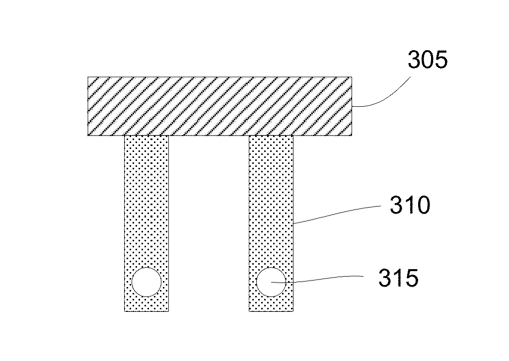
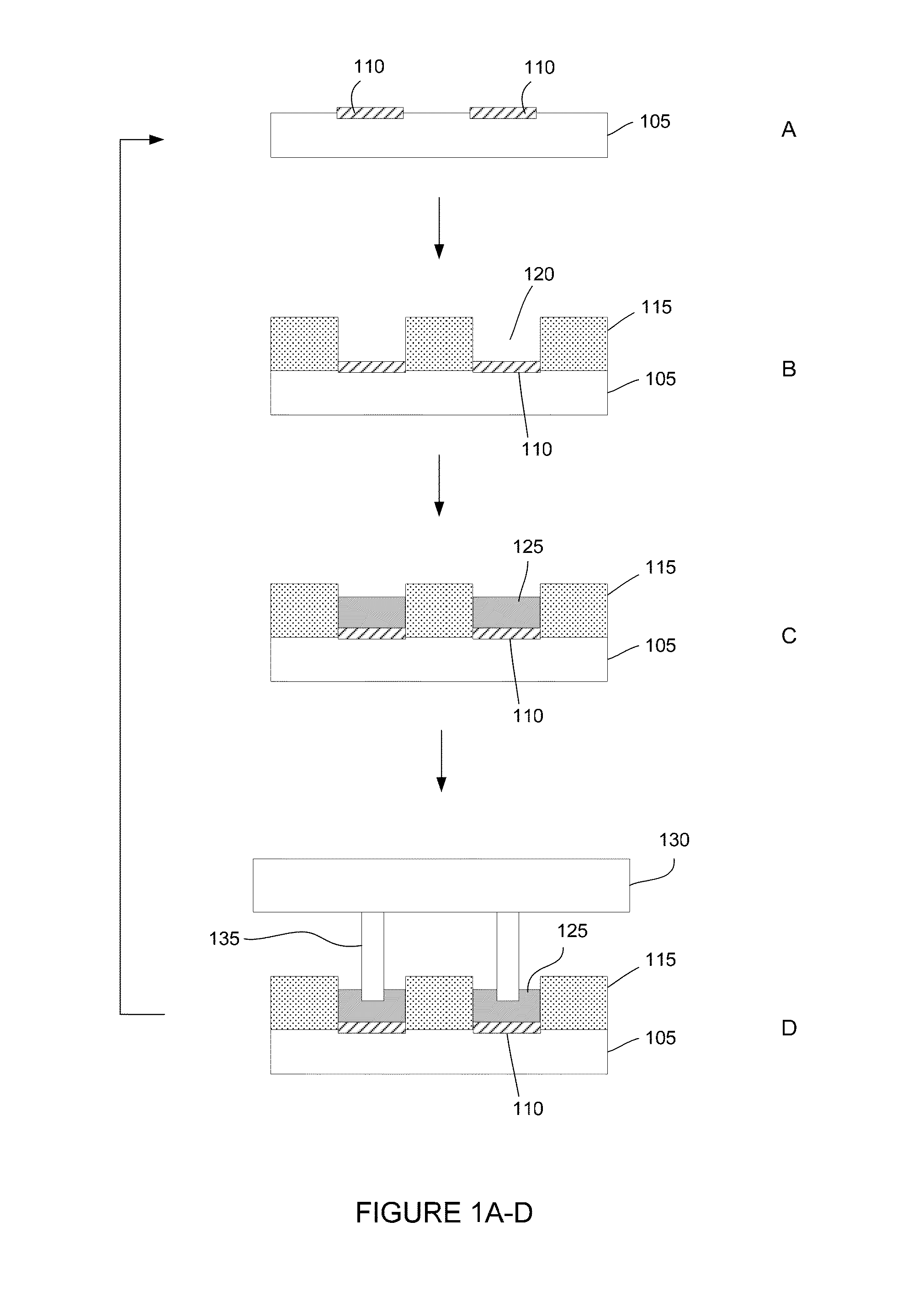
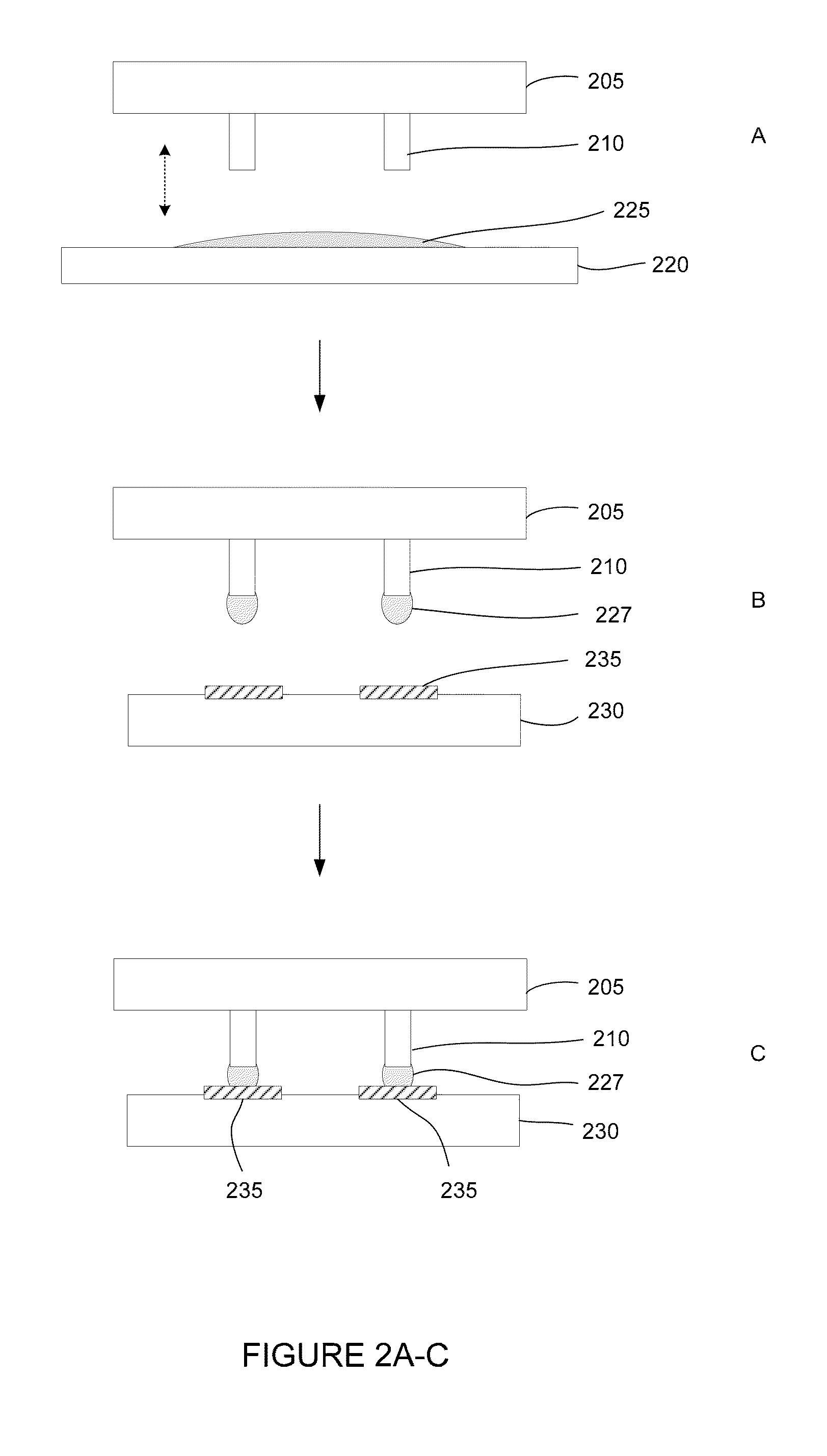
[0010]Embodiments of the present invention provide interconnects that are useful for example, for the testing and validation of semiconductor devices. In embodiments of the invention, the interconnects are capable of delivering high currents, such as, currents larger than 1 A, and testing devices presenting interfaces with feature pitches of less than 90 μm. In embodiments of the invention, interconnects are comprised of gallium or liquid metal alloys of gallium. The use of liquid metal contacts does not require that a predetermined amount of force be applied between the testing interface and the device being tested in order to reliably make an electrical connection. By not applying a mechanical force during the formation of electrical connections for chip testing and validation, mechanical stresses on the solid members of the testing and validation system (such as the device under test) can be decoupled.

[0011]Embodiments of the invention are useful for high temperature testing and ...


PUM

PropertyMeasurementUnit
diameteraaaaaaaaaa
diameteraaaaaaaaaa
diameteraaaaaaaaaa

Abstract

Embodiments of the invention provide methods for forming electrical connections using liquid metals. Electrical connections that employ liquid metals are useful for testing and validation of semiconductor devices. Electrical connections are formed between the probes of a testing interface and the electronic interface of a device under test through a liquid metal region. In embodiments of the invention, liquid metal interconnects are comprised of gallium or liquid metal alloys of gallium. The use of liquid metal contacts does not require a predetermined amount of force be applied in order to reliably make an electrical connection.

Description

BACKGROUND OF THE INVENTION[0001]1. Field of the Invention[0002]The embodiments of the invention relate generally to integrated circuit devices, and more specifically to testing and validation of semiconductor chips, testing systems for semiconductor chips, liquid metal interconnects, and liquid metal alloys.[0003]2. Background Information[0004]The push for ever-smaller integrated circuits (IC) places enormous performance demands on the techniques and materials used to construct and test IC devices. In general, an integrated circuit chip is also known as a microchip, a silicon chip, a chip, or a die. IC chips are found in a variety of common devices, such as the microprocessors in computers, cars, televisions, CD players, and cellular phones. A plurality of IC chips are typically built on a wafer (for example, a thin silicon disk, having a diameter of 300 mm) and after processing the wafer is diced apart to create individual chips (dies or dice).[0005]As part of the manufacturing pr...

Claims


Application Information

Patent Timeline
Patent Type & Authority Applications(United States)
IPC IPC(8): H01R43/16
CPCH01R3/08Y10T29/49204G01R1/06783G01R1/0416
Inventor BASKARAN, RAJASHREEJUN, KIMINZHONG, TINGSWART, ROY E.FISCHER, PAUL B.
Owner INTEL CORP
Why Eureka
Try Eureka