Active device having variable energy/optical properties
a technology of optical properties and active devices, applied in non-linear optics, instruments, optics, etc., can solve the problems of film becoming hazy, their mechanical properties may be far inferior to those that may be required, and achieve the effect of avoiding a bending of the cover
- Summary
- Abstract
- Description
- Claims
- Application Information
AI Technical Summary
Benefits of technology
Problems solved by technology
Method used
Image
Examples
first embodiment
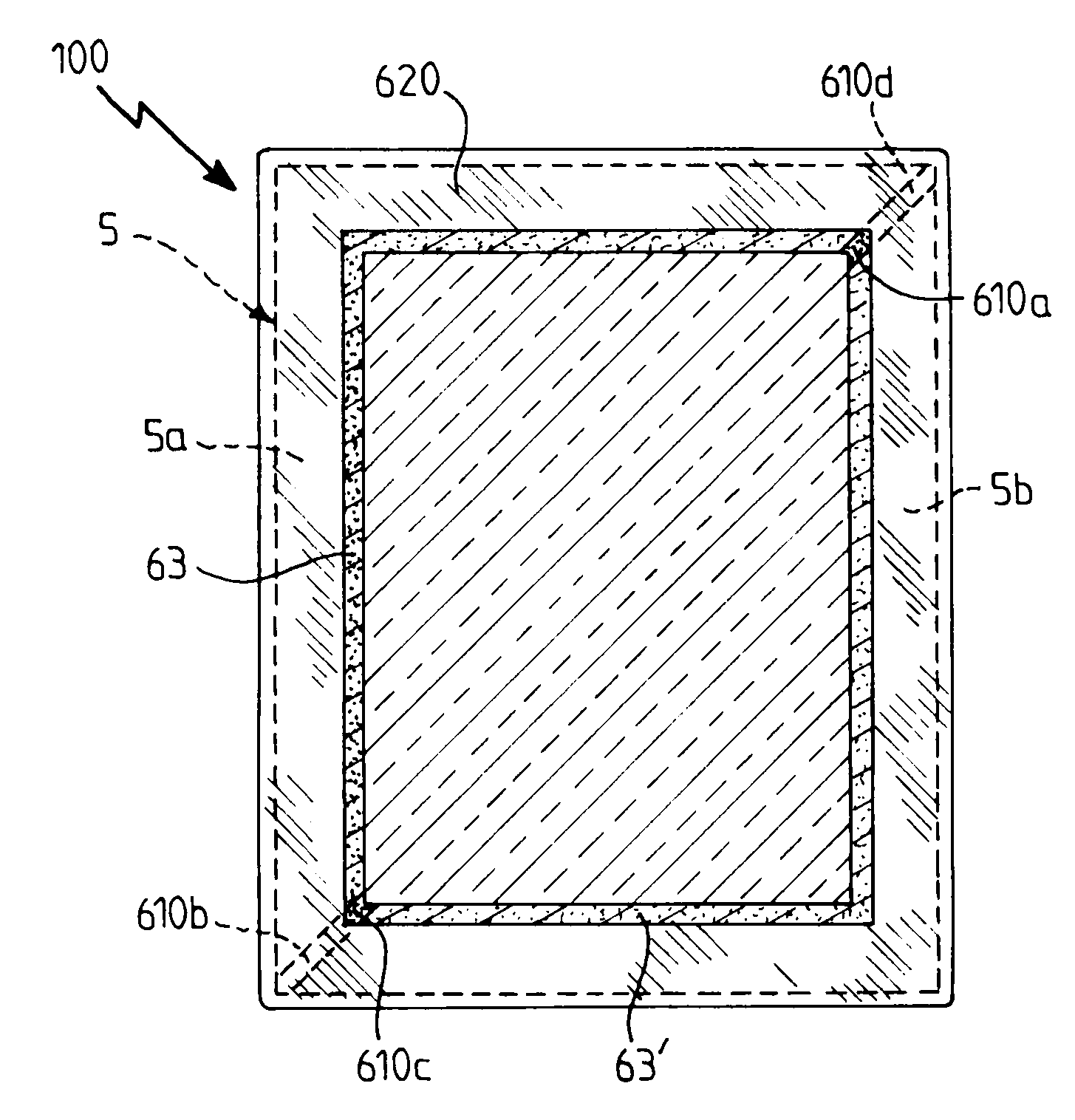
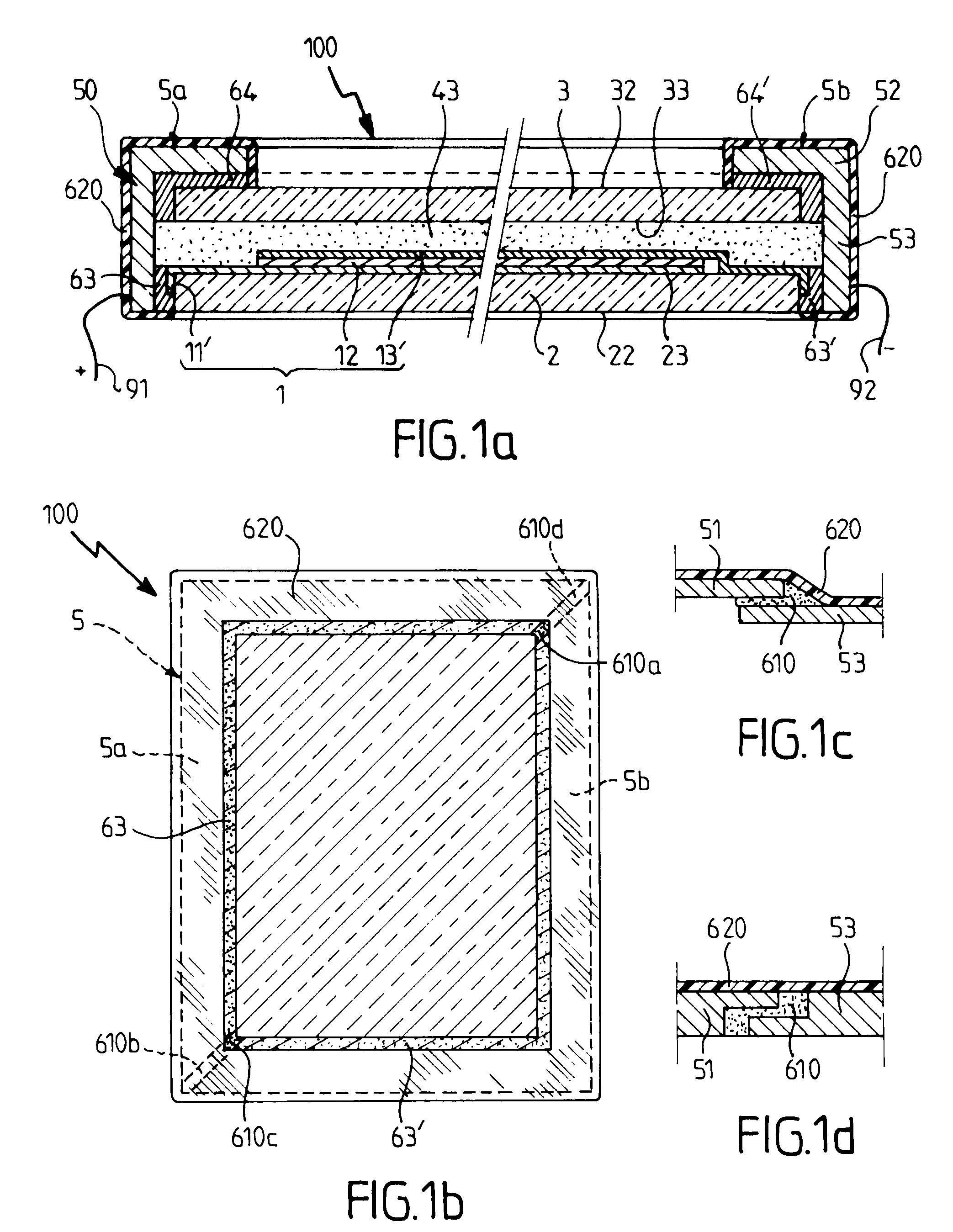
FIGS. 1a to 1d show partial schematic views in a side section and from below of an active device 100 in the invention.
The device 100 is an inorganic electrochromic device comprising for example:a lower electrode 11 comprising a stack of layers of the type ITO / ZnO:Al / Ag / ZnO:Al / ITO having respective thicknesses of 15 to 20 nm for ITO / 60 to 80 nm for ZnO:Al / 3 to 15 nm for silver / 60 to 80 nm for ZnO:Al / 15 to 20 nm for ITO, or is based on ITO (indium tin oxide) having a thickness of 500 nm, hot deposited (350° C.),an active stack 12 formed froma first layer of anode electrochromic material of indium oxide (hydrate) of 40 to 100 nm or of nickel oxide hydrate of 40 to 400 nm, alloyed or not with other metals, such as cobalt, rhenium, rhodium,a first electrolyte layer preferably made from tungsten oxide having a thickness of 100 nm or of silicone nitride optionally alloyed with aluminum or boron, boron nitride, aluminum nitride,a second electrolyte layer of tantalum oxide hydrate or silicon...
second embodiment
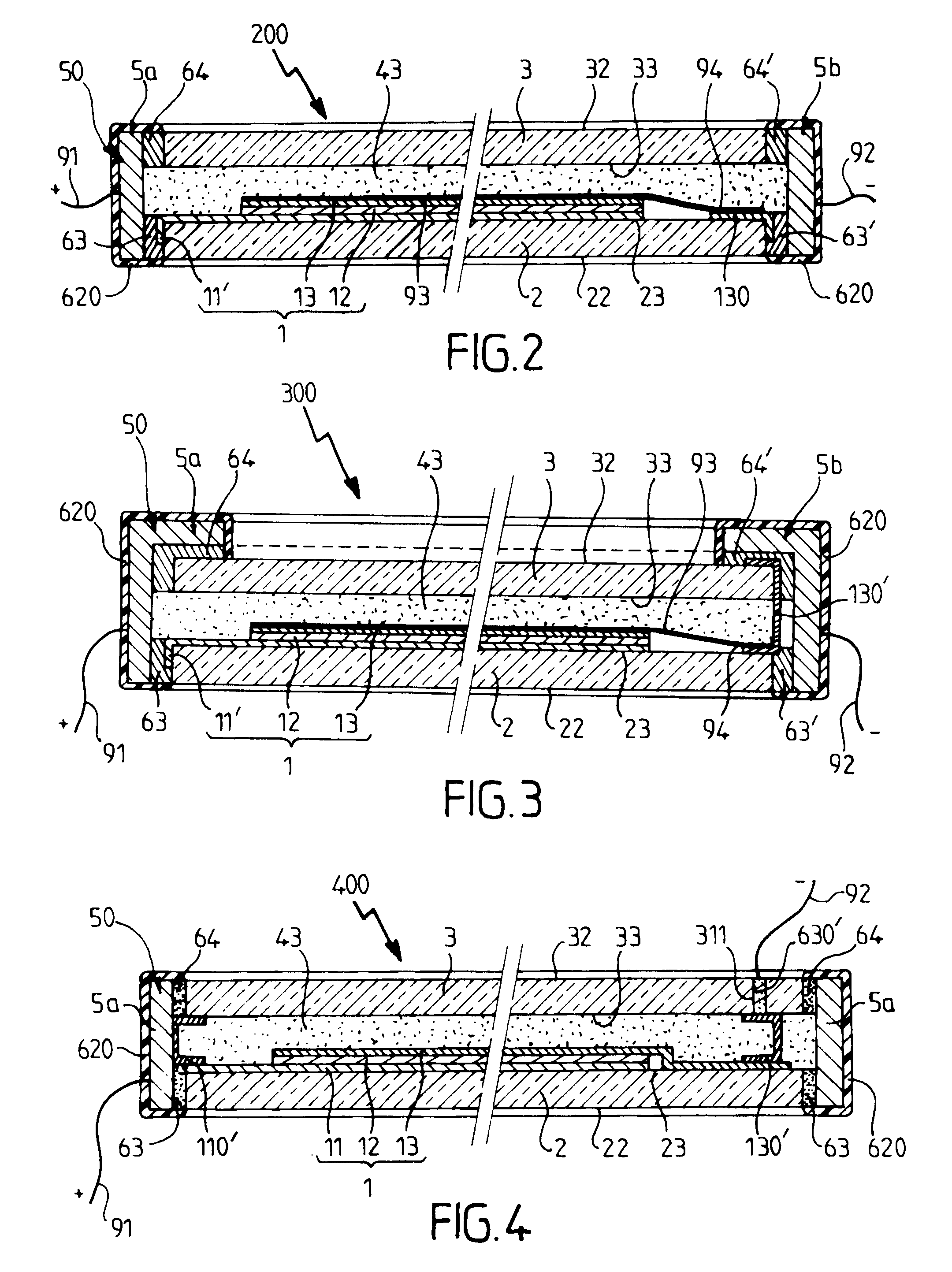
FIG. 2 shows a schematic cross section of an active device 200 in the invention.
This second device 200 differs from the device 100 by the features described below.
The upper electrode 13 does not extend on the substrate. It is associated with other conductive elements, for example a layer more conductive than itself, and / or with a plurality of conductive strips or wires. For further detail, reference can be made to patent WO-00 / 57243 for the implementation of such “multicomponent electrodes”.
Thus to the upper electrode 13 (optionally surmounted by one or more other conductive layers) a network of conductive wires 93 may be applied (parallel, in a grid, etc.) encrusted on the surface of the lamination spacer 43.
The end 94 of the network of wires 93 serves to connect the upper electrode 13 to the metal weld 63′ via a conductive zone which is preferably a “busbar” type strip 130 of conductive silver enamel, for example deposited by screen printing, and about 10 to 100 μm thick, or even ...
third embodiment
FIG. 3 shows a schematic cross section of an active device 300 in the invention.
This third device 300 differs from the preceding devices by the features described below mainly concerned with the internal connection means.
The end 94 of the network of wires 93 serves to connect the upper electrode 13 to one of the metal welds 64′ of the cover 3 via a U-shaped foil type strip 130′ of tin-plated copper. This foil 130′ has:a portion that is both (pre)fixed—for example by softening the spacer—against the spacer 43 and pressed or fastened—for example by weld or conductive cement particularly epoxy containing silver or by material deposited by inkjet loaded with metal (nano)particles such as silver or copper—to the inner border 23 of the substrate,a portion that is both (pre)fixed against the edge of the spacer 43, for example by softening the spacer, by pressed or fastened—for example by weld or conductive cement in particular epoxy containing silver or even by material deposited by inkjet...
PUM
| Property | Measurement | Unit |
|---|---|---|
| area | aaaaa | aaaaa |
| thickness | aaaaa | aaaaa |
| thickness | aaaaa | aaaaa |
Abstract
Description
Claims
Application Information


