
Milling of Granular Silicon

a technology of granular silicon and milling, which is applied in the direction of grain treatment, silicon, etc., can solve the problems of high cost of silicon parts, high cost of conventional monocrystalline silicon wafers, and ineffective and widespread use as economical replacements for commercial power, etc., to achieve high purity, control the size, and economic and reliable effects

Inactive Publication Date: 2013-01-17
INTEGRATED PHOTOVOLTAICS
View PDF0 Cites 28 Cited by
  • Summary
  • Abstract
  • Description
  • Claims
  • Application Information

AI Technical Summary

Benefits of technology

This patent describes a way to make very pure and very small silicon particles. The process involves mechanically grinding silicon particles down to a specific size, or jet milling them into a powder that can be sprayed onto things using plasma. This method is cost-effective and reliable, and can produce high-quality silicon powder.

Problems solved by technology

Solar cells can also be made in such wafers, but the conventional monocrystalline silicon wafers are generally considered to be too expensive for solar cells to be effectively and widely deployed as an economical replacement for commercial power.
Although the parts can be easily replaced with new silicon parts, silicon parts are generally expensive.

Method used


Image

  • Milling of Granular Silicon
  • Milling of Granular Silicon
  • Milling of Granular Silicon

Examples


Embodiment Construction

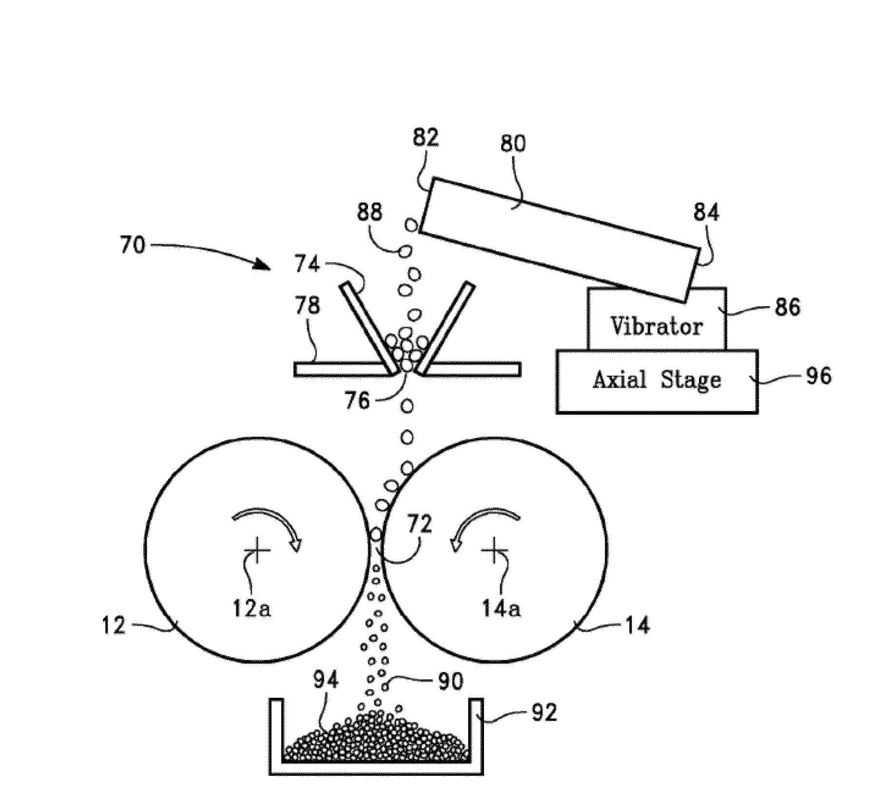
[0022]Different aspects of the invention include mechanical grinding or crushing of silicon pieces to small particles of high purity and of controlled size. Mechanical grinding may be followed by an optional sieving and subsequent jet milling of the particles into yet smaller silicon powder. However, the silicon feedstock must be highly pure and the purity must be maintained during the grinding process.

[0023]The semiconductor industry has promoted the development of economical production of electronic grade silicon (EGS) of very high purity. In the usual Siemens process, gaseous precursors of hydrogen and trichlorosilane are injected into a reactor containing a hot seed rod of silicon. The precursors in a chemical vapor deposition (CVD) process deposit onto the seed rod as growing layers of polysilicon silicon to form a rod or ingot or boule of EGS, also called virgin polysilicon. The growth conditions favor the formation of high stress in the ingots. At the end of growth, the ingot...


PUM


Abstract

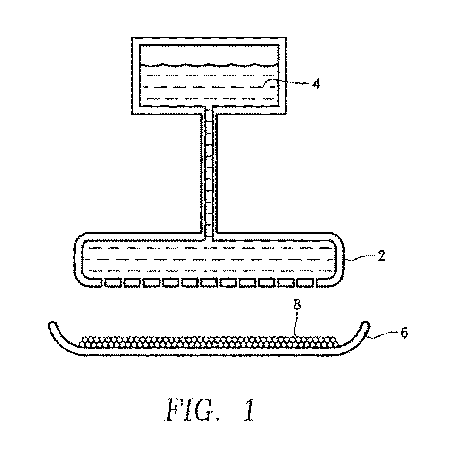
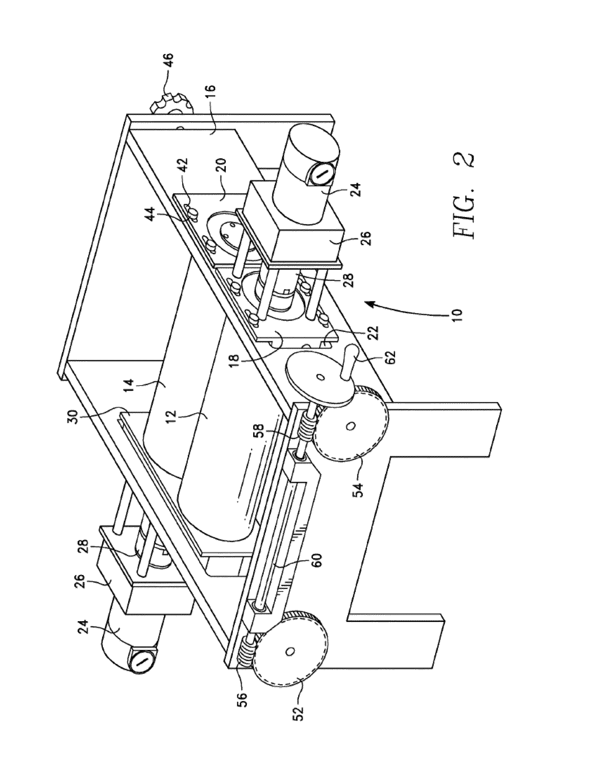
Silicon particles, including powder suitable for plasma spraying semiconductor devices, is formed by milling by a roller mill including silicon rollers and / or plates and having feed and collection systems comprising silicon and operated in a controlled ambient.

Description

PRIORITY[0001]This application is a continuation-in-part and claims priority from U.S. application Ser. No. 12 / 749,160, filed Mar. 29, 2010 and U.S. 61 / 165,218 filed Mar. 31, 2009.CROSS-REFERENCE TO RELATED APPLICATIONS[0002]This application is related in part to U.S. application Ser. Nos. 12 / 074,651, 12 / 720,153, 12 / 749,160, 12 / 789,357, 12 / 860,048, 12 / 950,725, 12 / 860,088, 13 / 010,700, 13 / 019,965, 13 / 073,884, 13 / 104,881, 13 / 214,158, 13 / 234,316 and U.S. Pat. No. 7,789,331, all owned by the same assignee and incorporated by reference in their entirety herein. Additional technical explanation and background is cited in the referenced material.FIELD OF THE INVENTION[0003]The invention relates generally to producing silicon powder useful for plasma spraying semiconducting devices such as solar cells. In particular, the invention relates to milling of silicon particles with a mill comprising silicon components.BACKGROUND ART[0004]Integrated circuits based upon semiconducting silicon have co...

Claims


Application Information

Patent Timeline
IPC IPC(8): B02C17/00B02C1/08
CPCB02C4/02B02C4/283C01B33/02B02C4/30B02C4/286
Inventor ZEHAVI, RAANAN Y.
Owner INTEGRATED PHOTOVOLTAICS
Learn More