TSV structure and method for forming the same

Inactive Publication Date: 2013-01-17
UNITED MICROELECTRONICS CORP
View PDF45 Cites 33 Cited by
  • Summary
  • Abstract
  • Description
  • Claims
  • Application Information

AI Technical Summary

Benefits of technology

[0010]The present invention as a result proposes a novel method to make a novel through-silicon via structure as well as a novel through-silicon via structure. The novel through-silicon via structure of the present invention is a seamless through-silicon via structure. Because there is no conventional silicon sandwiched between the conductive layer and the inner wall of the through via, a through-silicon via structure of smaller size maybe obtained even though the size of the conductive material layer is no

Problems solved by technology

However, the conductive material must bear high temperatures.
To be viewed as a whole, the filling of copper is particularly difficult and there is possible contamination of copper because the CMOS is co

Method used


Image

  • TSV structure and method for forming the same
  • TSV structure and method for forming the same
  • TSV structure and method for forming the same

Examples


Example

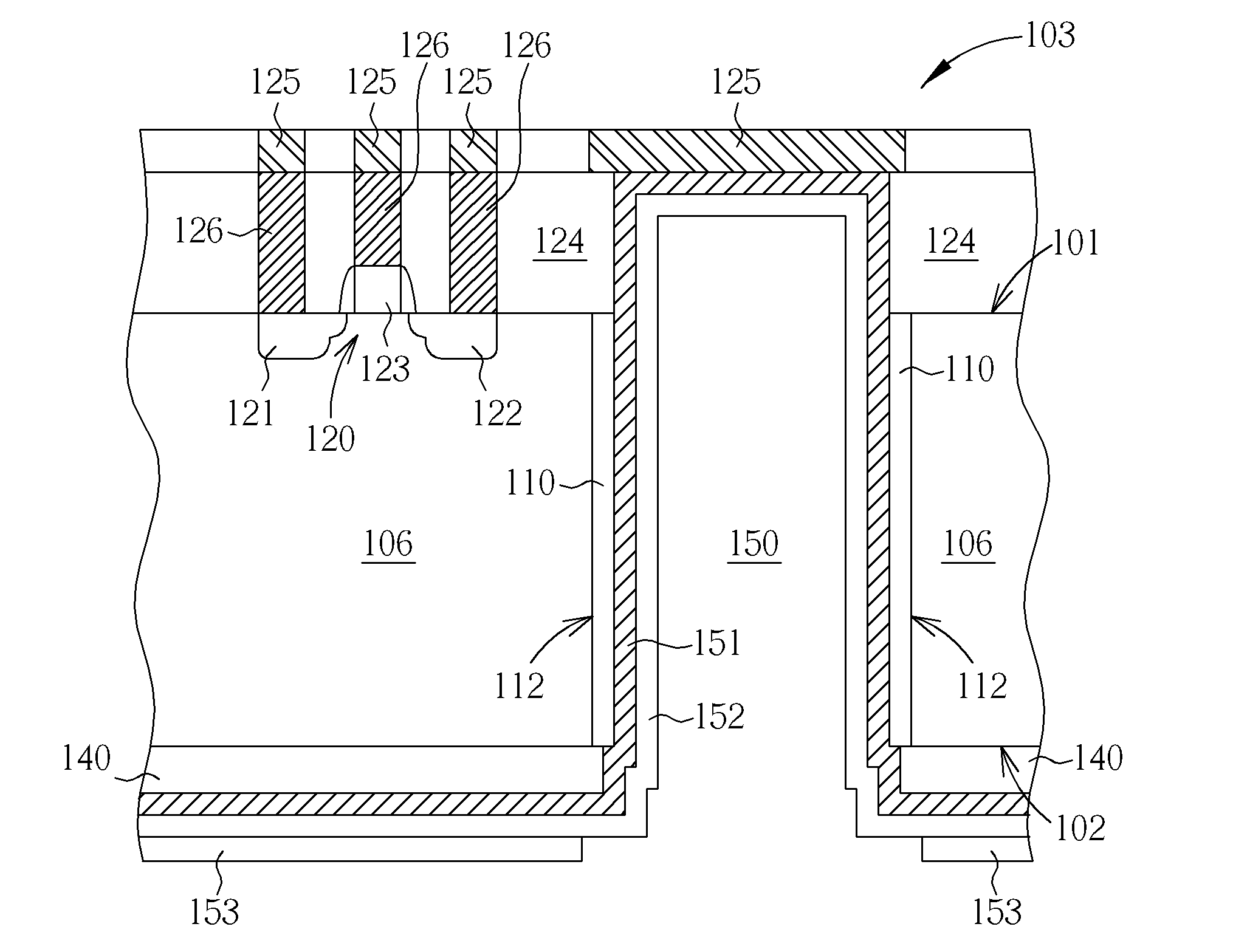
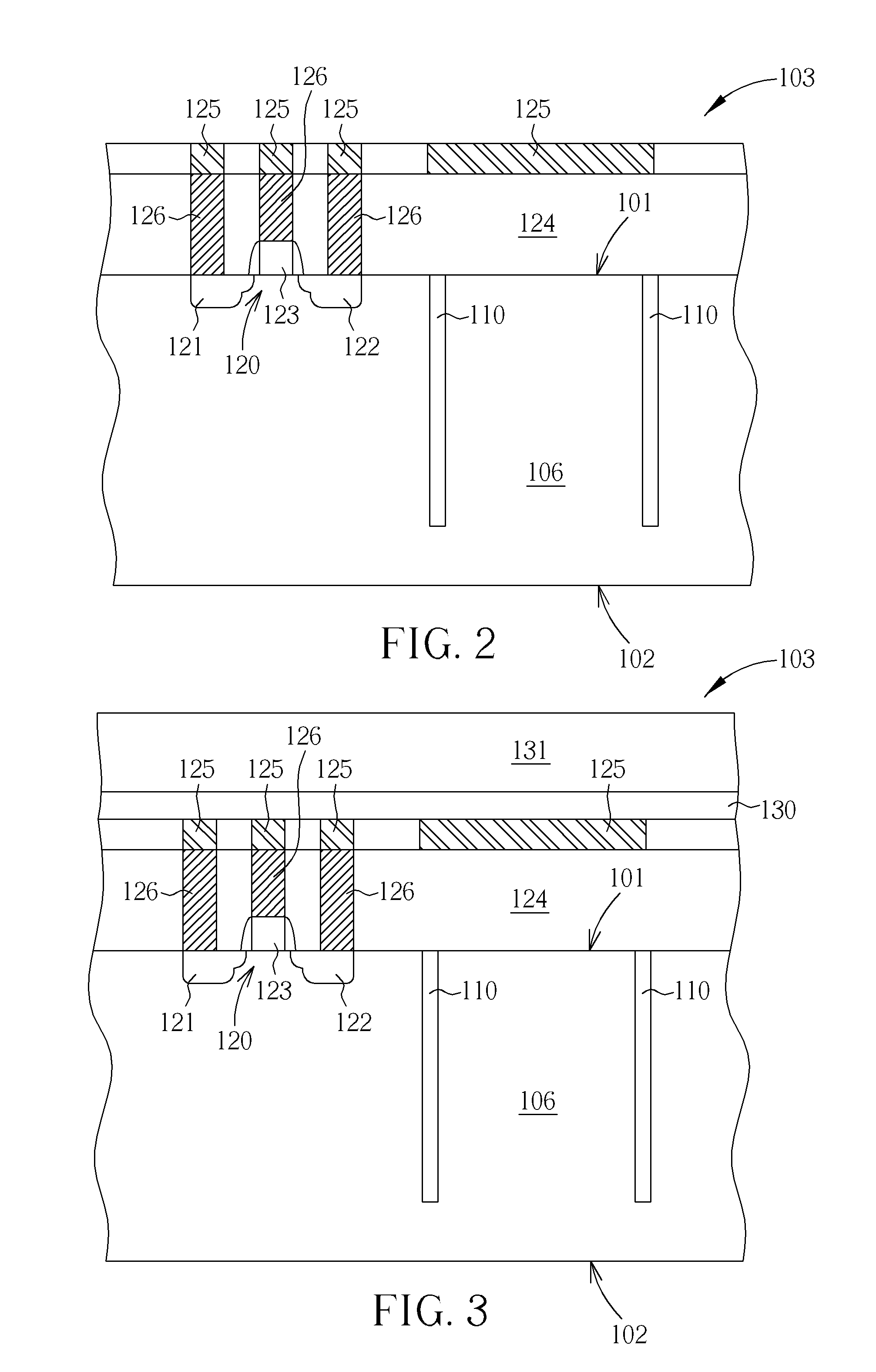
[0020]Second, in a first embodiment, an annular dielectric layer 110 is formed in the wafer 103. The annular dielectric layer 110 may be formed along with the formation of the shallow trench isolation (not shown). For example, lithographic and etching steps may be used to form recesses (not shown) in the wafer 103 to respectively define the annular dielectric layer 110 and the shallow trench (not shown). The size of the openings on the reticle and etching recipes may be used to control the depth of the recesses and the shallow trenches. Preferably, the depth of the recesses should be deeper than that of the shallow trenches. Later, a dielectric material, such as silicon oxide, may be used to fill the recesses and the shallow trenches, followed by planarization to respectively obtain the annular dielectric layer 110 and the shallow trench isolation (not shown). Optionally, the ring thickness of the annular dielectric layer 110 may be 2 μm-3 μm.

Example

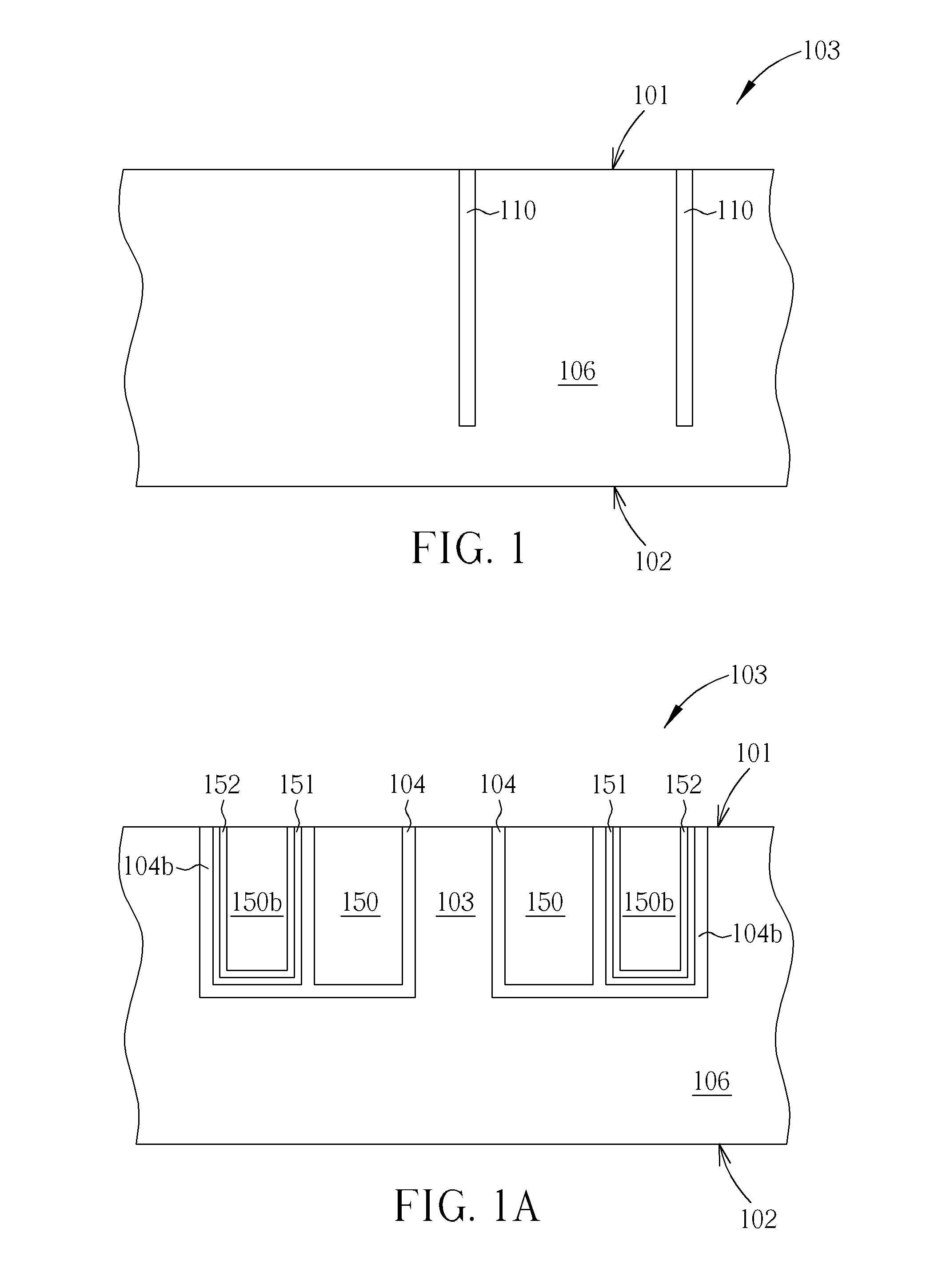
[0021]Please refer to FIG. 1A, in a second embodiment a recess (not shown) is etched in the wafer 103 to accommodate the through via dielectric ring, a first conductive ring and a first dielectric ring which are formed in later steps. The recess (not shown) maybe formed along with the formation of the shallow trench isolation (not shown). After the recess (not shown) is formed, an isolation layer 104 is formed on the inner wall of the recess (not shown) and later a conductive material fills the recess (not shown) to form a conductive layer 150, such as by deposition to fill up the recess (not shown). After the isolation layer 104 and the conductive layer 150 are done, some of the substrate in the wafer 103 is disposed between the isolation layer 104 and the conductive layer 150.

[0022]Before the conductive layer 150 fills the recess (not shown), at least one of a barrier layer (not shown) and a seed layer (not shown) may be optionally formed on the inner wall of the isolation layer 1...


PUM


Abstract

A TSV structure includes a wafer including a first side and a second side, a through via connecting the first side and the second side, a through via dielectric layer covering the inner wall of the through via, a conductive layer which fills up the through via and consists of a single material to be a seamless TSV structure, a first dielectric layer covering the first side and surrounding the conductive layer as well as a second dielectric layer covering the second side and part of the through via dielectric layer but partially covered by the conductive layer.

Description

BACKGROUND OF THE INVENTION[0001]1. Field of the Invention[0002]The present invention generally relates to a TSV (through-silicon via) structure and the method for forming the TSV structure. In particular, the present invention generally relates to a method to fall into the formation of the TSV structure after the formation of CMOSs and to form a through via dielectric layer before the formation of CMOSs in order to avoid the problems of BEOL jeopardizing the TSV structure to cause pumping and to avoid the problem of copper contamination owing to wafer thinning.[0003]2. Description of the Prior Art[0004]The through-silicon via technique is a quite novel semiconductor technique. The through-silicon via technique mainly resides in solving the problem of the electrical interconnection of chips and belongs to anew 3D packing field. The hot through-silicon via technique creates the products which better meet the market trends of “light, thin, short and small” by the 3D stacking through t...

Claims


Application Information

Patent Timeline
IPC IPC(8): H01L23/48H01L29/06H01L21/768H01L29/772
CPCH01L21/84H01L27/0694H01L27/12H01L21/76898H01L23/481H01L2224/05H01L2224/02372H01L2924/1461H01L2224/03H01L2224/05548H01L2224/13024H01L2224/0401H01L2924/00
Inventor KUO, CHIEN-LIYANG, CHIN-SHENGLIN, MING-TSE
Owner UNITED MICROELECTRONICS CORP
Why Eureka
Try Eureka