Conversion Gain Modulation Using Charge Sharing Pixel

a charge sharing and conversion gain technology, applied in the field of image sensors, can solve the problems of reducing sensitivity, reducing pixel fill factor, and limited low light sensitivity, and achieve the effect of low conversion gain and high conversion gain

Active Publication Date: 2013-01-24
PIXIM
View PDF5 Cites 49 Cited by
  • Summary
  • Abstract
  • Description
  • Claims
  • Application Information

AI Technical Summary

Problems solved by technology

For large size pixels, low light sensitivity can be limited by the CG of the FD.
Therefore, the pixel will suffer from low CG in low light conditions, leading to reduced sensitivity, particularly in low light conditions.
However, this method requires two additional elements (transistor M5 and capacitor C5) added to the pixel circuit and so reduces the pixel fill factor (reducing sensitivity and photodiode full well).

Method used


Image

  • Conversion Gain Modulation Using Charge Sharing Pixel
  • Conversion Gain Modulation Using Charge Sharing Pixel
  • Conversion Gain Modulation Using Charge Sharing Pixel

Examples


first embodiment

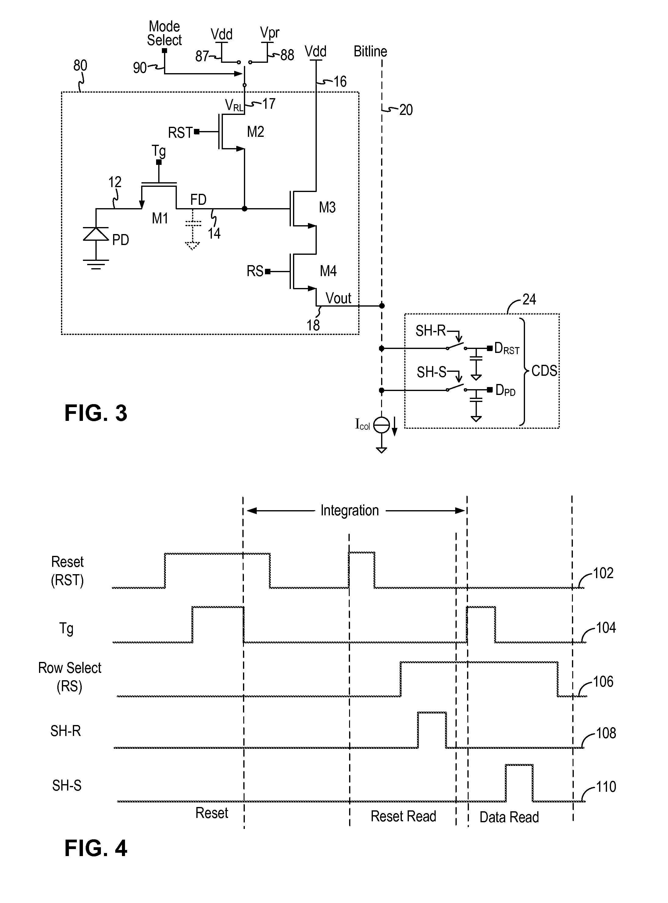
[0052]In a first embodiment, a first CSM operating mode (Mode A1) is configured for single read out per frame with the transfer gate signal Tg set low during integration and set high during readout.

[0053]FIG. 8 is a timing diagram for CSM Operation Mode A1, utilizing single readout, with the transfer gate set low during the integration time according to one embodiment of the present invention. Under Mode A1 operation, a partial reset is performed by asserting the reset signal RST (curve 102) to turn on the reset transistor and asserting the transfer gate signal Tg (curve 104) to turn on the transfer gate transistor. The reset level voltage VRL is set to the partial reset voltage (curve 103). Accordingly, the photodiode and the floating diffusion are reset to the same potential which is a voltage value that is slightly less than the pinning voltage of the photodiode.

[0054]Light integration begins when the reset signal RST is deasserted. The transfer gate Tg remains asserted to allow ...

second embodiment

[0058]In a second embodiment, a second CSM operating mode (Mode A2) is configured for single readout with the transfer gate signal Tg set high during integration and read out.

[0059]FIG. 9 is a timing diagram for CSM Operation Mode A2, utilizing single readout, with the transfer gate set high during integration and readout according to one embodiment of the present invention. Under Mode A2 operation, a partial reset is performed by asserting the reset signal RST (curve 102) to turn on the reset transistor and asserting the transfer gate signal Tg (curve 104) to turn on the transfer gate transistor. The reset level voltage VRL is set to the partial reset voltage (curve 103). Accordingly, the photodiode and the floating diffusion are reset to the same potential which is a voltage value that is slightly less than the pinning voltage of the photodiode.

[0060]Light integration begins when the reset signal RST is deasserted. The transfer gate Tg remains asserted to allow the reset voltage v...

third embodiment

[0065]In a third embodiment, a third CSM operating mode (Mode A3) is configured for single readout with the transfer gate signal Tg set low during integration and read out.

[0066]FIG. 10 is a timing diagram for CSM Operation Mode A3, utilizing single readout, with the transfer gate set low during integration and readout according to one embodiment of the present invention. Under Mode A2 operation, a partial reset is performed followed by the reset read operation. The transfer gate signal Tg is deasserted after the partial reset and before the reset read. Light integration starts when the transfer gate signal is deasserted until the data read operation. Following integration, the transfer gate signal Tg is pulsed high to transfer charge from the photodiode to the floating diffusion. When the photodiode PD and the floating diffusion FD have reached a new potential equilibrium, the transfer gate Tg is deasserted, and the floating diffusion FD is read out during the data read period.

[006...


PUM


Abstract

An image sensor including an array of pixel elements is operated according to two operation modes to modulate the conversion gain of the pixel to operate the image sensor based on the impinging light conditions. More specifically, an image sensor pixel element is operated in a high conversion gain mode for low light conditions and in a low conversion gain mode for bright light conditions. The low conversion gain mode implements charge sharing between the floating diffusion and the photodiode. The low conversion gain mode further implements partial reset where the photodiode and the floating diffusion are reset to the same potential and to a potential slightly less than the pinning voltage of the photodiode.

Description

CROSS-REFERENCE TO RELATED APPLICATIONS[0001]This application claims the benefit of U.S. Provisional Patent Application Ser. No. 61 / 429,162, filed on Jan. 2, 2011, which application is incorporated herein by reference in its entirety.FIELD OF THE INVENTION[0002]The invention relates to image sensors and, in particular, to image sensors with multiple conversion gain settings.DESCRIPTION OF THE RELATED ART[0003]CMOS image sensor pixel circuits formed using four transistors are known and are referred to as 4T image sensor pixels or “4T pixels.” In 4T CMOS image sensor pixels, the photodiode (PD) provides the photon to electron conversion, while the floating diffusion (FD) provides the electron to voltage conversion. The voltage per electron conversion of the FD is known as conversion gain (CG) and is an important parameter for CMOS image sensors. Conversion gain boosts the pixel signal relative to the analog noise, thereby reducing the noise floor, and thereby enabling performance at l...

Claims


Application Information

Patent Timeline
Patent Type & Authority Applications(United States)
IPC IPC(8): H01L27/146
CPCH01L27/14609H01L27/14683H04N5/355H04N5/374H04N5/243H04N5/3537H04N5/3559H04N25/57H04N25/59H04N23/76H04N25/76H04N25/534
Inventor AYERS, THOMASBRADY, FREDERICK THOMASKANG, JINSUKHWANG, SUNGINYU, SEN
Owner PIXIM
Why Eureka
Try Eureka