Silicon carbide substrate, semiconductor device, and methods for manufacturing them
a technology of silicon carbide substrate and semiconductor device, which is applied in the direction of fine working device, semiconductor device, electrical apparatus, etc., can solve the problems of device increase and yield reduction, and achieve the effect of reducing on-resistance and improving the yield of semiconductor devi
- Summary
- Abstract
- Description
- Claims
- Application Information
AI Technical Summary
Benefits of technology
Problems solved by technology
Method used
Image

Examples
first embodiment
[0052]Firstly, a first embodiment as one embodiment of the present invention will be described. Referring to FIG. 1, a silicon carbide substrate 1 in the present embodiment is entirely made of single-crystal silicon carbide, and in one main surface 1A, sulfur atoms are present at not less than 60×1010 atoms / cm2 and not more than 2000×1010 atoms / cm2, and oxygen atoms are present at not less than 3 at % and not more than 30 at %.
[0053]Since presence ratios of the sulfur atoms and the oxygen atoms in main surface 1A of silicon carbide substrate 1 are set to not more than 2000×1010 atoms / cm2 and not more than 30 at %, respectively, even if an epitaxial growth layer is formed on main surface 1A, formation of a high-resistivity layer at an interface between the epitaxial growth layer and silicon carbide substrate 1 is suppressed due to the presence of the sulfur atoms and the oxygen atoms. Further, since a good-quality epitaxial growth layer can be formed on the silicon carbide substrate,...
second embodiment
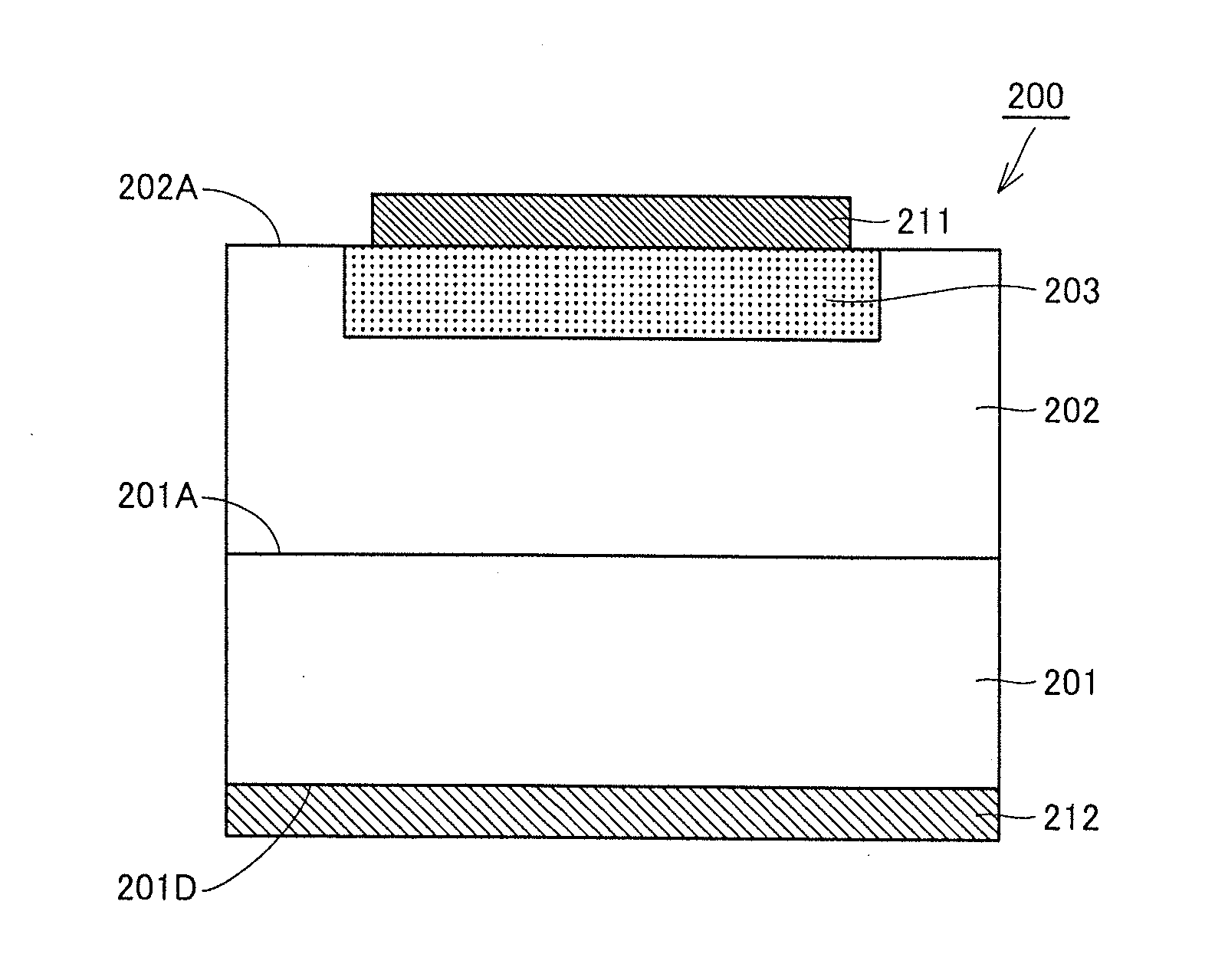
[0088]Next, a silicon carbide substrate in a second embodiment will be described. Referring to FIG. 10, silicon carbide substrate 1 in the second embodiment basically has the same structure and exhibits the same effect as those of silicon carbide substrate 1 in the first embodiment. However, silicon carbide substrate 1 in the second embodiment is different from that in the first embodiment in that it includes a base layer and a single-crystal silicon carbide layer.
[0089]Specifically, referring to FIG. 10, silicon carbide substrate 1 in the second embodiment includes a base layer 11, and a single-crystal silicon carbide layer 12 formed on base layer 11. Further, a main surface 12A of single-crystal silicon carbide layer 12 on a side opposite to a side facing base layer 11 corresponds to main surface 1A in the first embodiment. That is, in silicon carbide substrate 1 in the present embodiment, a region including one main surface 12A is made of single-crystal silicon carbide.
[0090]In s...
example 1
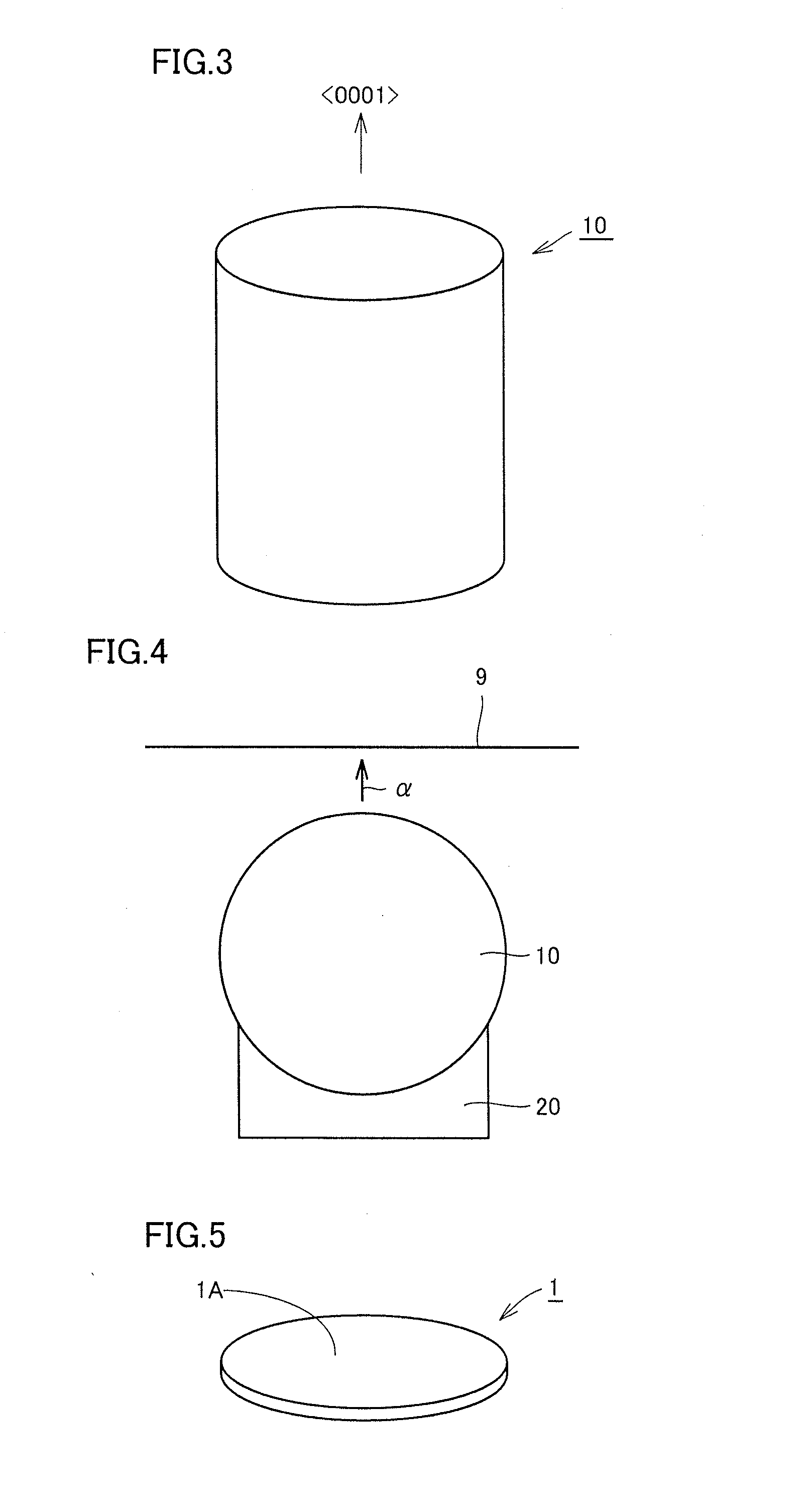
[0095]An experiment was conducted to investigate the influence of presence ratios of sulfur atoms and oxygen atoms in a main surface of a silicon carbide substrate on yield of devices. Specifically, 11 substrates having different presence ratios of sulfur atoms and oxygen atoms in main surfaces thereof were prepared, and a plurality of semiconductor devices were fabricated for each substrate. Then, operation of the fabricated devices was checked to investigate yield thereof. A silicon carbide single crystal was grown by the sublimation method. As a seed substrate, a silicon carbide substrate with a diameter of 50 mm having a main surface corresponding to a (0001) plane was used. The grown crystal had a nitrogen concentration of 1×1019 cm−3. A grown surface, a seed substrate surface, and an outer periphery of the crystal were ground with an outer periphery grinding machine to obtain a cylindrical ingot of silicon carbide. Slicing was performed using a multiwire saw. In order to obtai...
PUM
| Property | Measurement | Unit |
|---|---|---|
| surface roughness | aaaaa | aaaaa |
| diameter | aaaaa | aaaaa |
| off angle | aaaaa | aaaaa |
Abstract
Description
Claims
Application Information
 - Generate Ideas
- Intellectual Property
- Life Sciences
- Materials
- Tech Scout
- Unparalleled Data Quality
- Higher Quality Content
- 60% Fewer Hallucinations
Browse by: Latest US Patents, China's latest patents, Technical Efficacy Thesaurus, Application Domain, Technology Topic, Popular Technical Reports.
© 2025 PatSnap. All rights reserved.Legal|Privacy policy|Modern Slavery Act Transparency Statement|Sitemap|About US| Contact US: help@patsnap.com