Multilayer ceramic electronic component
- Summary
- Abstract
- Description
- Claims
- Application Information
AI Technical Summary
Benefits of technology
Problems solved by technology
Method used
Image

Examples
first preferred embodiment
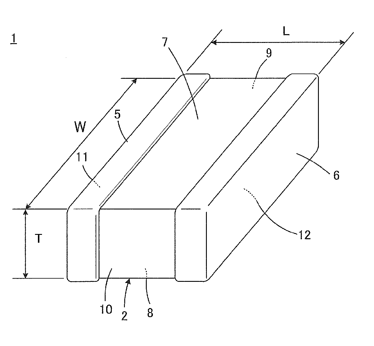
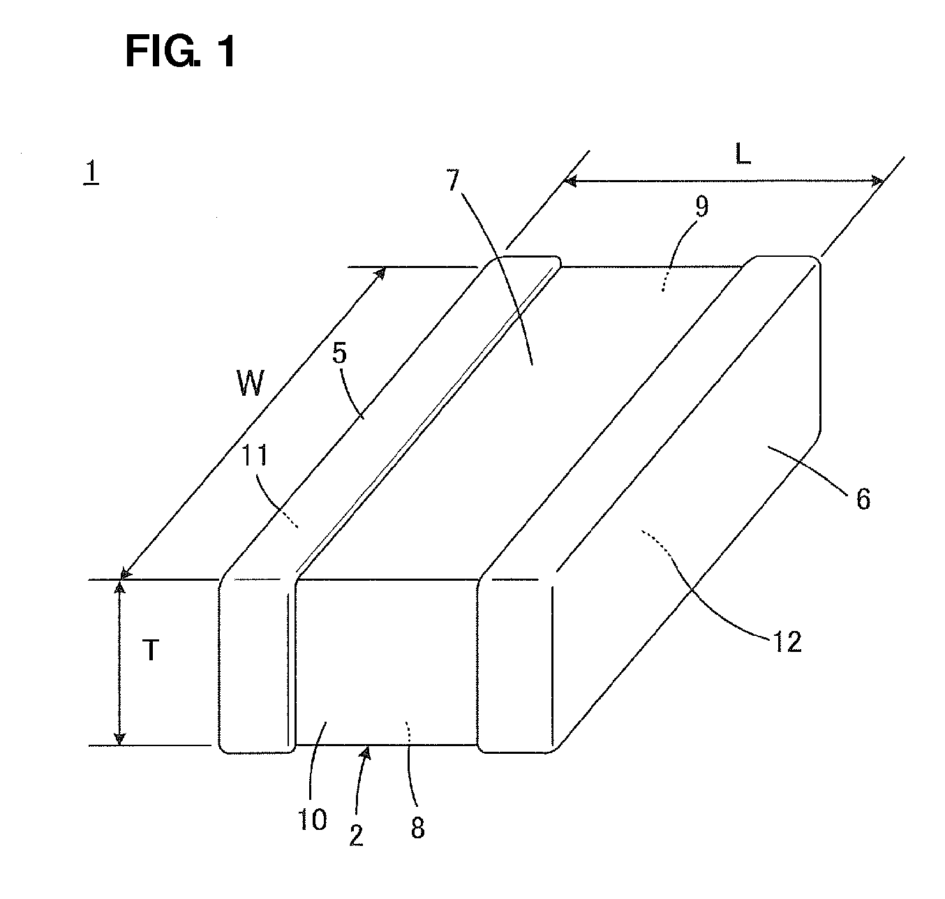
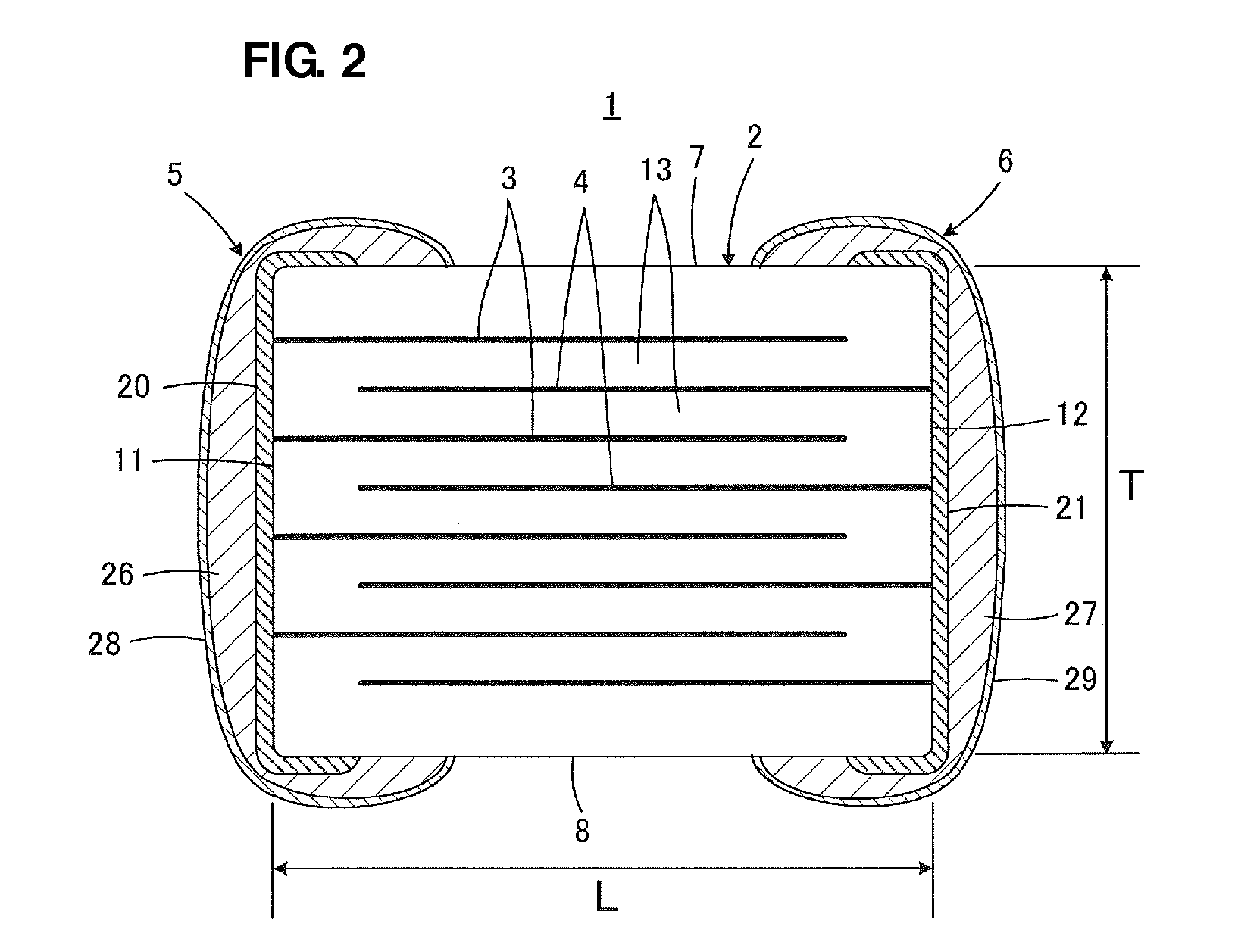
[0051]FIGS. 1 to 6 will be used to describe a first preferred embodiment of the present invention. A multilayer ceramic capacitor 1 according to the first preferred embodiment is an ESR controlling capacitor. The multilayer ceramic capacitor 1 includes a ceramic body 2, internal electrodes 3 and 4, which are arranged inside the ceramic body 2, and external electrodes 5 and 6, which are arranged on outer surfaces of the ceramic body 2. Hereafter, the structure of the multilayer ceramic capacitor 1 will be described in detail by separately describing the ceramic body, the internal electrodes, and the external electrodes. After that, a method of manufacturing the multilayer ceramic capacitor 1 will be described.
[0052]As illustrated in FIGS. 1 to 5, the ceramic body 2 preferably has a substantially rectangular parallelepiped shape including a pair of opposing principal surfaces 7 and 8, a pair of opposing side surfaces 9 and 10, and a pair of opposing end surfaces 11 and 12. It is prefe...
second preferred embodiment
[0103]A second preferred embodiment of the present invention is illustrated in FIG. 7. FIG. 7 corresponds to FIG. 3B. In FIG. 7, elements corresponding to those illustrated in FIG. 3B are denoted by the same reference symbols and repetitious description thereof will be omitted.
[0104]In a multilayer ceramic capacitor 1a illustrated in FIG. 7, protruding portions 22a to 25a are arranged so as to wrap around not only the end surfaces 11 and 12 but also so as to wrap around onto at least the side surfaces 9 and 10. Although not illustrated, the protruding portions 22a to 25a may be arranged so as to wrap around onto the principal surfaces 7 and 8.
[0105]With this configuration, although moisture may more easily penetrate to the protruding portions 22a to 25a, even if moisture does penetrate to the protruding portions 22a to 25a, since the exposed ends 16 and 19 of the internal electrodes 3 and 4 are not positioned underneath the protruding portions 22a to 25a, this is not a serious probl...
third preferred embodiment
[0106]A third preferred embodiment of the present invention is illustrated in FIG. 8. FIG. 8 corresponds to FIG. 4. In FIG. 8, elements corresponding to those illustrated in FIG. 4 are denoted by the same reference symbols and repetitious description thereof will be omitted.
[0107]A first conductive portion 20b and protruding portions 22b and 23b are disposed only on the end surface 11 of the ceramic body 2 illustrated in FIG. 8. Regarding a first conductive portion and protruding portions on the rear surface side, that is, the end surface 12 of the ceramic body 2 illustrated in FIG. 8, although not illustrated, they are provided only on the end surface 12.
[0108]With this configuration, the thickness of the external electrodes in the direction T (refer to FIG. 1 and FIG. 2) can be restrained and therefore the profile of the multilayer ceramic electronic component can be reduced.
PUM
| Property | Measurement | Unit |
|---|---|---|
| Thickness | aaaaa | aaaaa |
| Electrical conductor | aaaaa | aaaaa |
| Width | aaaaa | aaaaa |
Abstract
Description
Claims
Application Information
 - R&D Engineer
- R&D Manager
- IP Professional
- Industry Leading Data Capabilities
- Powerful AI technology
- Patent DNA Extraction
Browse by: Latest US Patents, China's latest patents, Technical Efficacy Thesaurus, Application Domain, Technology Topic.
© 2024 PatSnap. All rights reserved.Legal|Privacy policy|Modern Slavery Act Transparency Statement|Sitemap