Eureka AIR delivers breakthrough ideas for toughest innovation challenges, trusted by R&D personnel around the world.

Solutions for netlist reduction for multi-finger devices

Active Publication Date: 2013-01-24
GLOBALFOUNDRIES US INC
View PDF3 Cites 8 Cited by
  • Summary
  • Abstract
  • Description
  • Claims
  • Application Information

AI Technical Summary

Benefits of technology

The patent text describes a computer-implemented method for reducing the size of a netlist for a multi-finger semiconductor device. The method involves extracting a netlist for the device, identifying common nodes, and replacing all the fingers of the device with a new device having a total width equivalent to a sum of the widths of the fingers. The method also involves combining resistive, inductive, and capacitive elements at each common node to produce a reduced netlist. The technical effect of this invention is to improve the efficiency of layout extraction for multi-finger devices by reducing the size of the netlist.

Problems solved by technology

However, inclusion of parasitic elements in the netlist may increase the processing time and computation cost associated with the simulation, thereby complicating the design and simulation process.
While some netlist elements (e.g., interconnect resistive elements and interconnect capacitive elements) can be reduced using approaches known in the art (e.g., Δ-Y transformation or delta-star transformation, filtering, delay-oriented local operations, mathematical model order reduction, etc.), a netlist for multi-finger devices is difficult to effectively reduce, as it contains a netlisting of multiple MOS transistors (i.e., multiple model calls of MOS transistors).

Method used


Image

  • Solutions for netlist reduction for multi-finger devices
  • Solutions for netlist reduction for multi-finger devices
  • Solutions for netlist reduction for multi-finger devices

Examples


Embodiment Construction

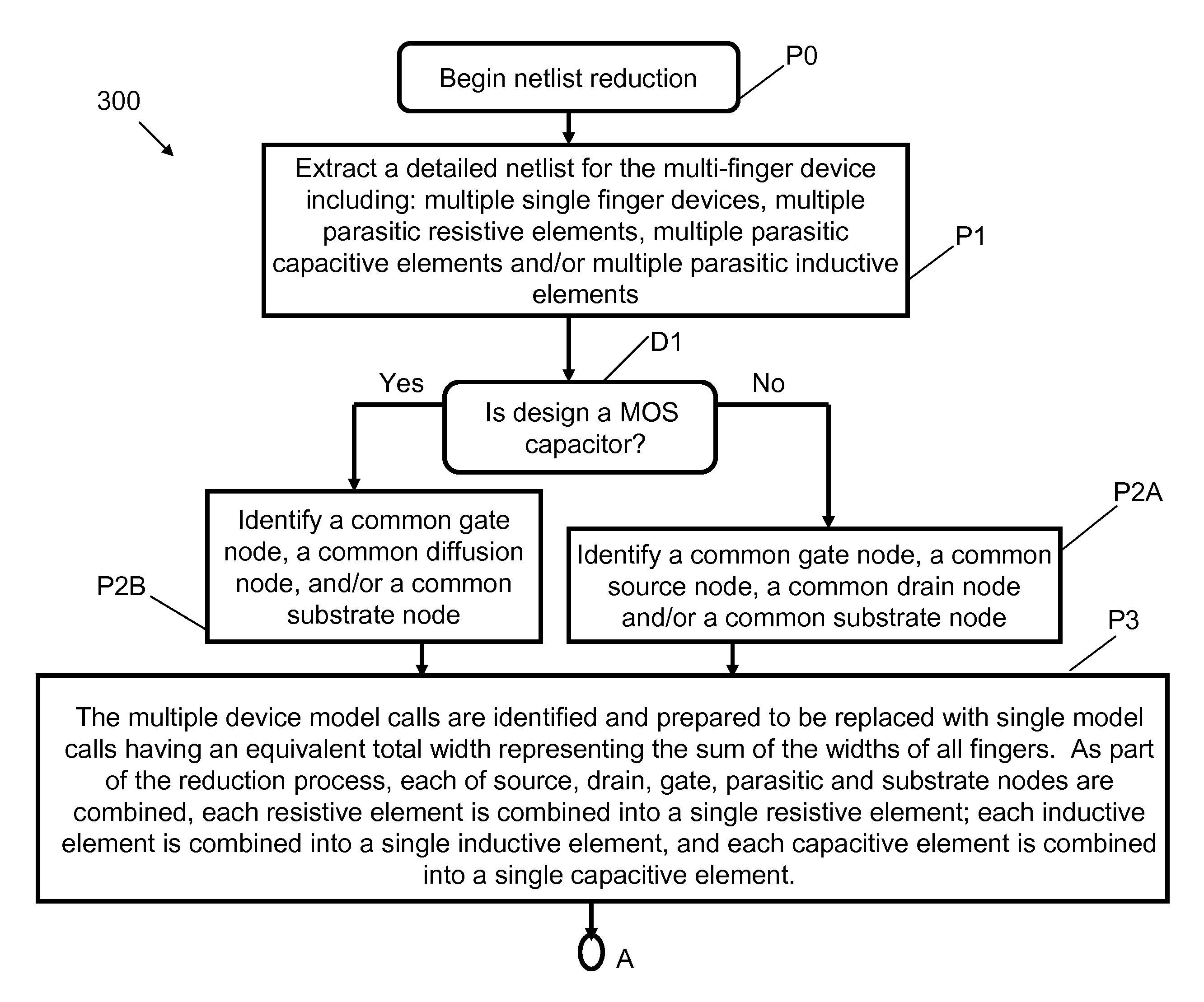
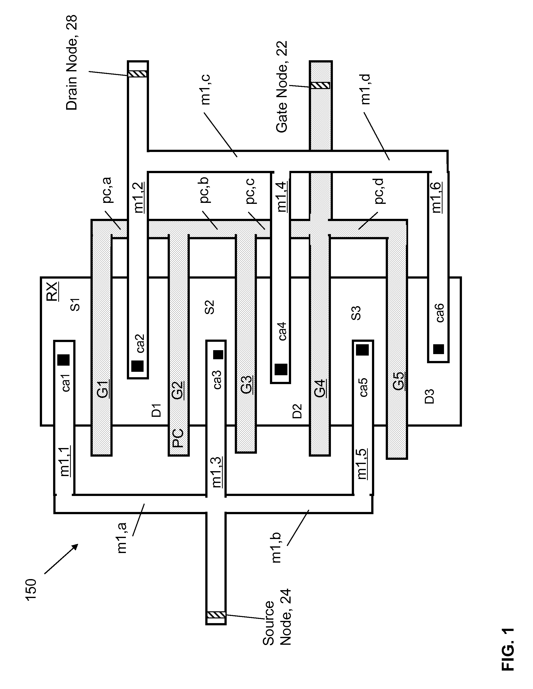
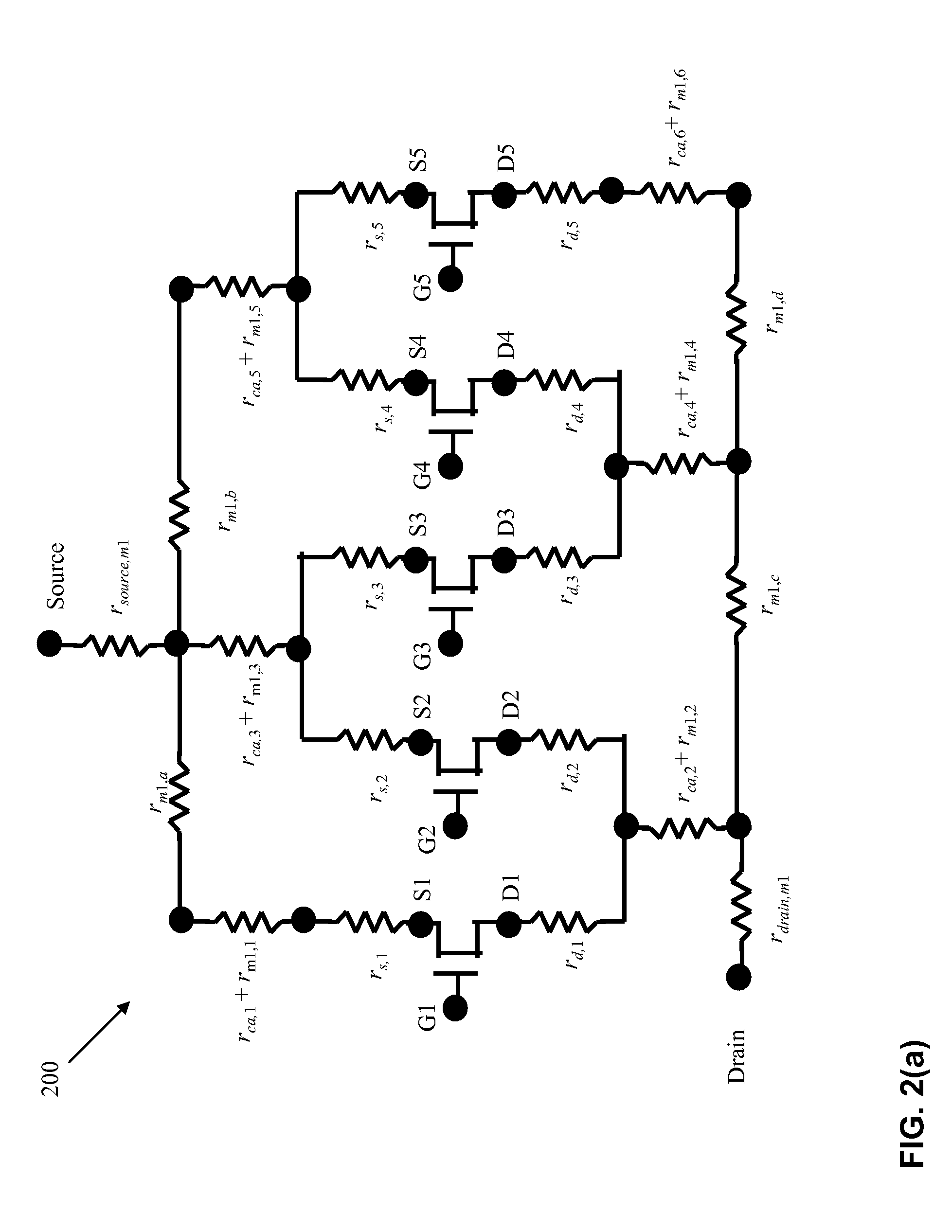
[0024]The subject matter disclosed herein relates to the analysis of integrated circuits, logic gates and / or multi-finger semiconductor devices, such as multi-finger metal-oxide-semiconductor (MOS) transistors, multi-finger MOS capacitors, etc. Specifically, the subject matter disclosed herein relates to solutions for netlist reduction for multi-finger devices.

[0025]In large-scale layout design, prior to producing devices, gates and / or circuits; simulations of the designs of these devices are run to improve the design, satisfy design rules and to optimize performance. These simulations may include the use of a netlist which represents the effects (e.g., resistance, capacitance, inductance, etc.) that various elements and the interconnections between the various elements have on the design / device.

[0026]In order to receive accurate simulation results for the design, parasitic elements must be included in the netlist which is to be simulated. These parasitic elements are extracted from...


PUM


Abstract

A computer-implemented method for performing a layout extraction for a multi-fingered semiconductor device is disclosed. The method reduces the netlist for the device and the number of device fingers by identifying a set of device common nodes, and combining a plurality of parasitic elements in the device to form a set of representative parasitic elements which are connected to respective device common nodes. In one embodiment, the method includes: extracting a netlist for the multi-finger device which includes a plurality of parasitic elements identifying a set of common nodes; replacing the fingers of the multi-finger device with a new device having a width equivalent to the widths of the fingers of the multi-finger device; and combining the parasitic elements of at least one device common node into a single representative parasitic element which is representative of the original parasitic elements.

Description

BACKGROUND OF THE INVENTION[0001]The subject matter disclosed herein relates to the analysis of integrated circuits, logic gates and / or multi-finger semiconductor devices, such as multi-finger metal-oxide-semiconductor (MOS) transistors, multi-finger MOS capacitors, etc. Specifically, the subject matter disclosed herein relates to solutions for netlist reductions of a multi-finger device.[0002]The design process for a semiconductor device, a logic gate or an integrated circuit may include computer implemented transistor-level circuit layout simulations. These simulations may include a Simulation Program with Integrated Circuit Emphasis (SPICE) netlist which includes the parasitic resistive elements (e.g., diffusion resistance, contact resistances, local wire resistance, etc.), parasitic capacitive elements (capacitive coupling between a transistor's gate and source, capacitive coupling between a transistor's gate and drain, capacitive coupling between a transistor's source and drain...

Claims


Application Information

Patent Timeline
IPC IPC(8): G06F9/45
CPCG06F17/5068G06F30/39
Inventor LU, NING
Owner GLOBALFOUNDRIES US INC
Why Eureka
Eureka Blog
Learn More