Ferroelectric device

Inactive Publication Date: 2013-02-07
PANASONIC INTELLECTUAL PROPERTY MANAGEMENT CO LTD
View PDF7 Cites 26 Cited by
  • Summary
  • Abstract
  • Description
  • Claims
  • Application Information

AI Technical Summary

Benefits of technology

[0014]It is an object of the present invention to provide a ferroelectric device, in which the crystallinity and

Problems solved by technology

Then, such a PZT thin film has poor quality of crystallinity and also has small piezoelectric constant e31, compared with a monocrystal PZT thin film formed on one surface side of a monocrystal MgO substrate or on one surface side of a monocrystal SrTiO3 substrate being more extremely-expensive than the silicon substrate.
However, the reality is that a PZT thin film having sufficient crystallinity has not yet been obtained.
However, when a functional portion that comprises a lower electrode, a ferroelectric film and an upper electrode is formed on one surface side of a silicon substrate and then a region of the silicon substrate corresponding to the functional port

Method used


Image

  • Ferroelectric device
  • Ferroelectric device
  • Ferroelectric device

Examples


first embodiment

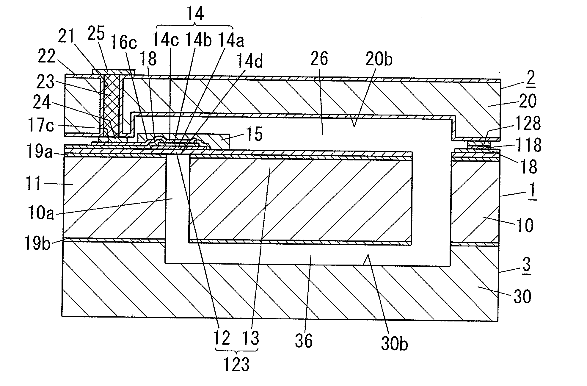
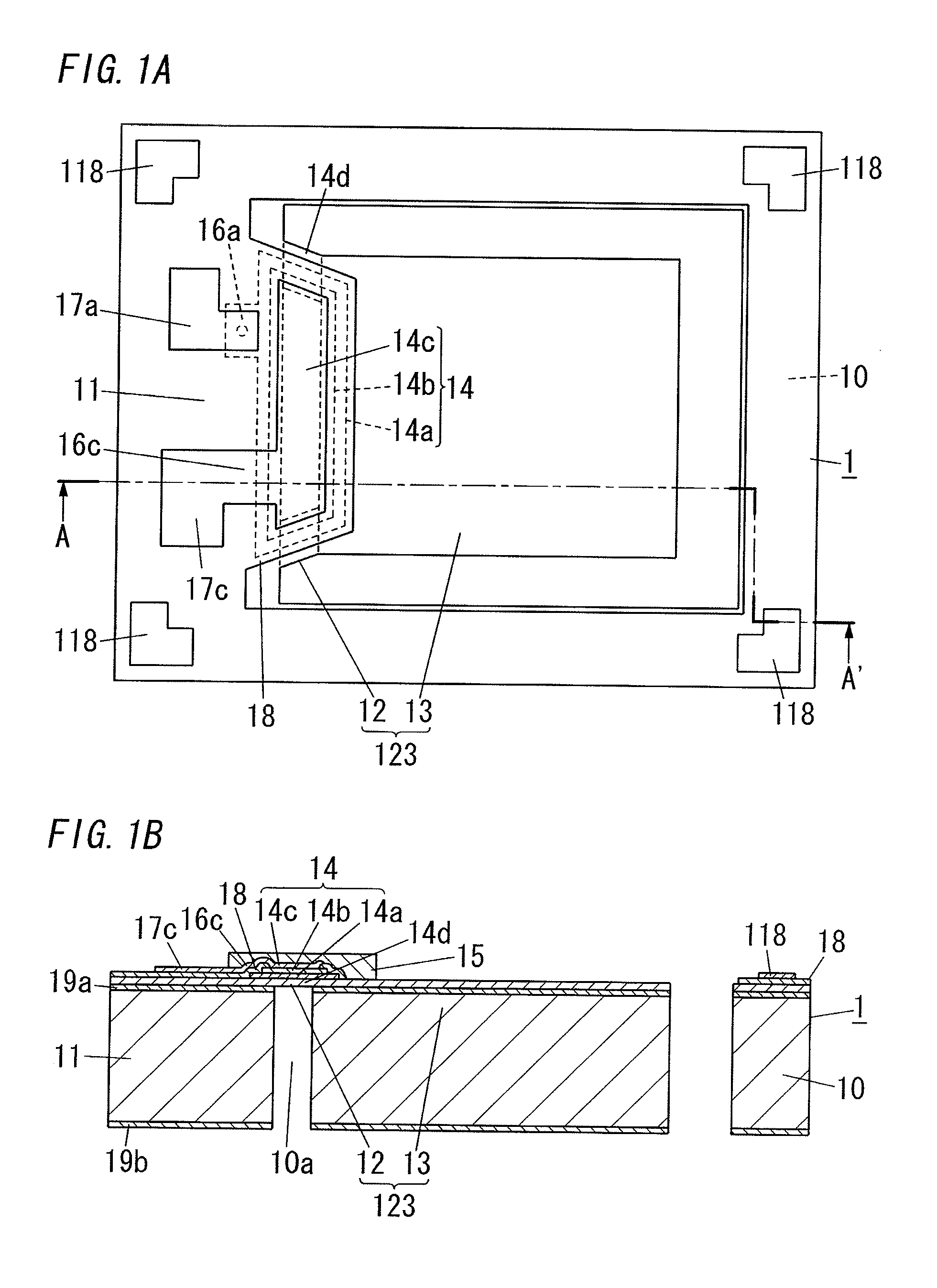
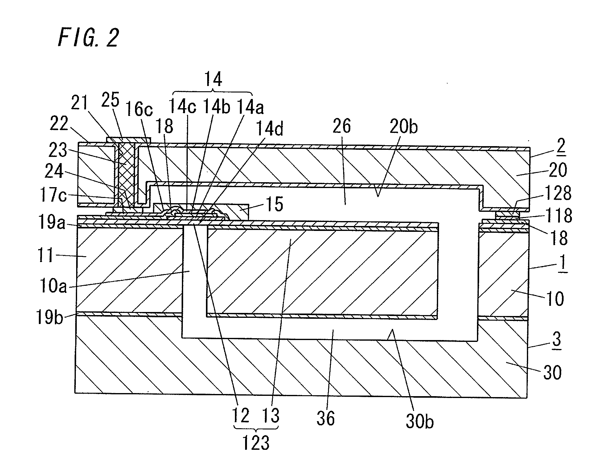
[0032]First, a ferroelectric device according to the present embodiment will be explained below referring to FIGS. 1A, 1B, 2 and 3.

[0033]A main unit 1 of the ferroelectric device comprises: a silicon substrate (hereinafter, called a first silicon substrate) 10; a first electrode 14a formed on one surface side of the first silicon substrate 10; a ferroelectric film 14b formed on a surface of the first electrode 14a opposite to the first silicon substrate 10 side; and a second electrode 14c formed on a surface of the ferroelectric film 14b opposite to the first electrode 14a side. That is, in FIG. 1B, the first electrode 14a is located on a lower surface side of the ferroelectric film 14b, as a lower electrode. The second electrode 14c is located on an upper surface side of the ferroelectric film 14b, as an upper electrode. Hereinafter, the first electrode 14a and the second electrode 14c are called the lower electrode 14a and the upper electrode 14c, respectively. Then, a monocrystal...

second embodiment

[0066]The basic configuration of a ferroelectric device of the present embodiment is substantially identical to that of the First Embodiment. As shown FIG. 4, the difference therebetween is that a second shock absorbing layer 14e is provided between the ferroelectric film 14b and the lower electrode 14a, in addition to the shock absorbing layer 14d (hereinafter, called a first shock absorbing layer) provided directly below the lower electrode 14a. The second shock absorbing layer 14e is formed of a material with better lattice matching with the ferroelectric film 14b than the lower electrode 14a. Then, the constituent elements same as those of the First Embodiment are assigned with same reference numerals and the explanation thereof is herein omitted.

[0067]A method for manufacturing the ferroelectric device of the present embodiment is substantially identical to that explained in the First Embodiment. The difference therebetween is that the lower electrode 14a is formed on the entir...

third embodiment

[0069]A ferroelectric device according to the present embodiment will be explained below referring to FIG. 5.

[0070]A ferroelectric device of the present embodiment comprises: a silicon substrate 10; a lower electrode 14a formed on one surface side of the silicon substrate 10; a ferroelectric film 14b formed on a surface of the lower electrode 14a opposite to the silicon substrate 10 side; and an upper electrode 14c formed on a surface of the ferroelectric film 14b opposite to the lower electrode 14a side. In this case, a monocrystal silicon substrate is used as the silicon substrate 10 and the one surface of the silicon substrate 10 is formed with a (100) face. The ferroelectric film 14b is formed of a ferroelectric material with a lattice constant difference from Si. Then, in the ferroelectric device, the constituent elements same as those of the First Embodiment are assigned with same reference numerals.

[0071]The ferroelectric device of the present embodiment is a pyroelectric inf...


PUM


Abstract

A ferroelectric device comprises: a silicon substrate (a first substrate); a lower electrode (a first electrode) formed on one surface side of first substrate; a ferroelectric film formed on a surface of lower electrode opposite to first substrate side; and an upper electrode (a second electrode) formed on a surface of ferroelectric film opposite to lower electrode side. The ferroelectric film is formed of a ferroelectric material with a lattice constant difference from silicon. The ferroelectric device further comprises a shock absorbing layer formed of a material with better lattice matching with ferroelectric film than silicon and provided directly below the lower electrode. The first substrate is provided with a cavity that exposes a surface of shock absorbing layer opposite to lower electrode side.

Description

TECHNICAL FIELD[0001]The invention relates generally to ferroelectric devices and, more particularly, to a ferroelectric device that uses a piezoelectric effect or a pyroelectric effect of a ferroelectric film.BACKGROUND ART[0002]Conventionally, ferroelectric devices that use a piezoelectric effect or a pyroelectric effect of a ferroelectric film have been attracting attention.[0003]As an example of a ferroelectric device of this type, a MEMS (micro electro mechanical systems) device, that comprises a functional portion having a ferroelectric film in one surface side of a silicon substrate, has been proposed, from the viewpoint of the cost reduction, the mechanical strength and the like. As a MEMS device of this type, for example, a power generating device (for example, see R. van Schaijk, et al, “Piezoelectric AlN energy harvesters for wireless autonomoustransducer solutions”, IEEE SENSORS 2008 Conference, 2008, page 45-48) or an actuator that uses a piezoelectric effect of a ferro...

Claims


Application Information

Patent Timeline
IPC IPC(8): H01L29/84B81B7/02G01J1/02G01P15/09H01L41/08H01L41/113H01L41/18H01L41/187H01L41/22H01L41/23H01L41/319H01L41/39H02N2/18
CPCB81B2201/032B81C1/00658G01J5/04G01J5/046G01J5/34G01P2015/0828H01L41/0815H01L41/1136H02N2/186G01P15/09H01L37/02H10N15/10H10N30/10516H10N30/306G01J1/02H10N30/30
Inventor OGAWA, JUNYAYAMAUCHI, NORIHIROMATSUSHIMA, TOMOAKIAIZAWA, KOICHI
Owner PANASONIC INTELLECTUAL PROPERTY MANAGEMENT CO LTD
Why Eureka
Try Eureka