Wafer level package structure and the fabrication method thereof

a technology of wafer level and packaging structure, applied in the direction of semiconductor devices, semiconductor/solid-state device details, electrical devices, etc., can solve the problems of chip being fragile or lacking corners, prone to cracking, and prone to cracking

Active Publication Date: 2013-02-14
ALPHA & OMEGA SEMICON INC
View PDF2 Cites 92 Cited by
  • Summary
  • Abstract
  • Description
  • Claims
  • Application Information

AI Technical Summary

Problems solved by technology

However, the thinner the chip is, the more easily it cracks.
However, the actual fabrication processes have some issues, for example, singulation of the wafer easily causes the edge or corner of a chip to crack resulting in the chip being fragile or lacking the corner.
On the other hand, in most of the current wafer level chip scale packages some parts of the chip in the devices are exposed from the molding compo

Method used


Image

  • Wafer level package structure and the fabrication method thereof
  • Wafer level package structure and the fabrication method thereof
  • Wafer level package structure and the fabrication method thereof

Examples


Embodiment Construction

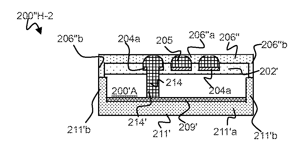
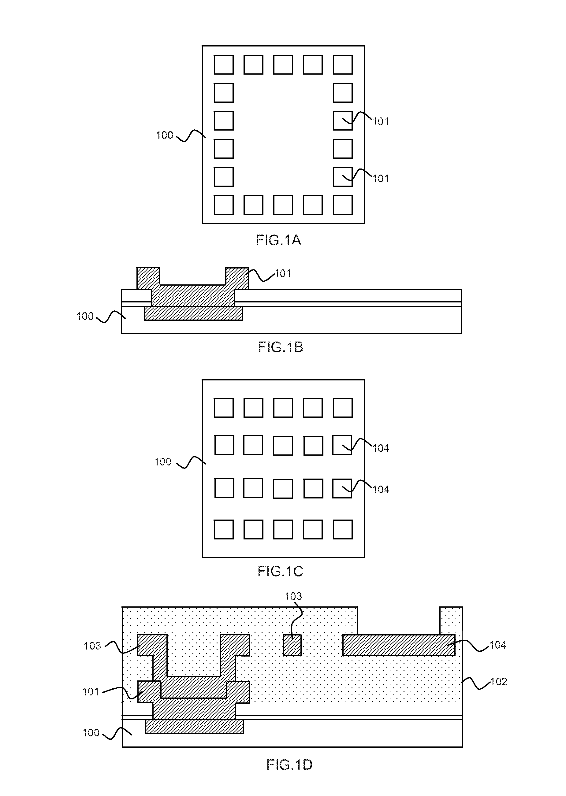
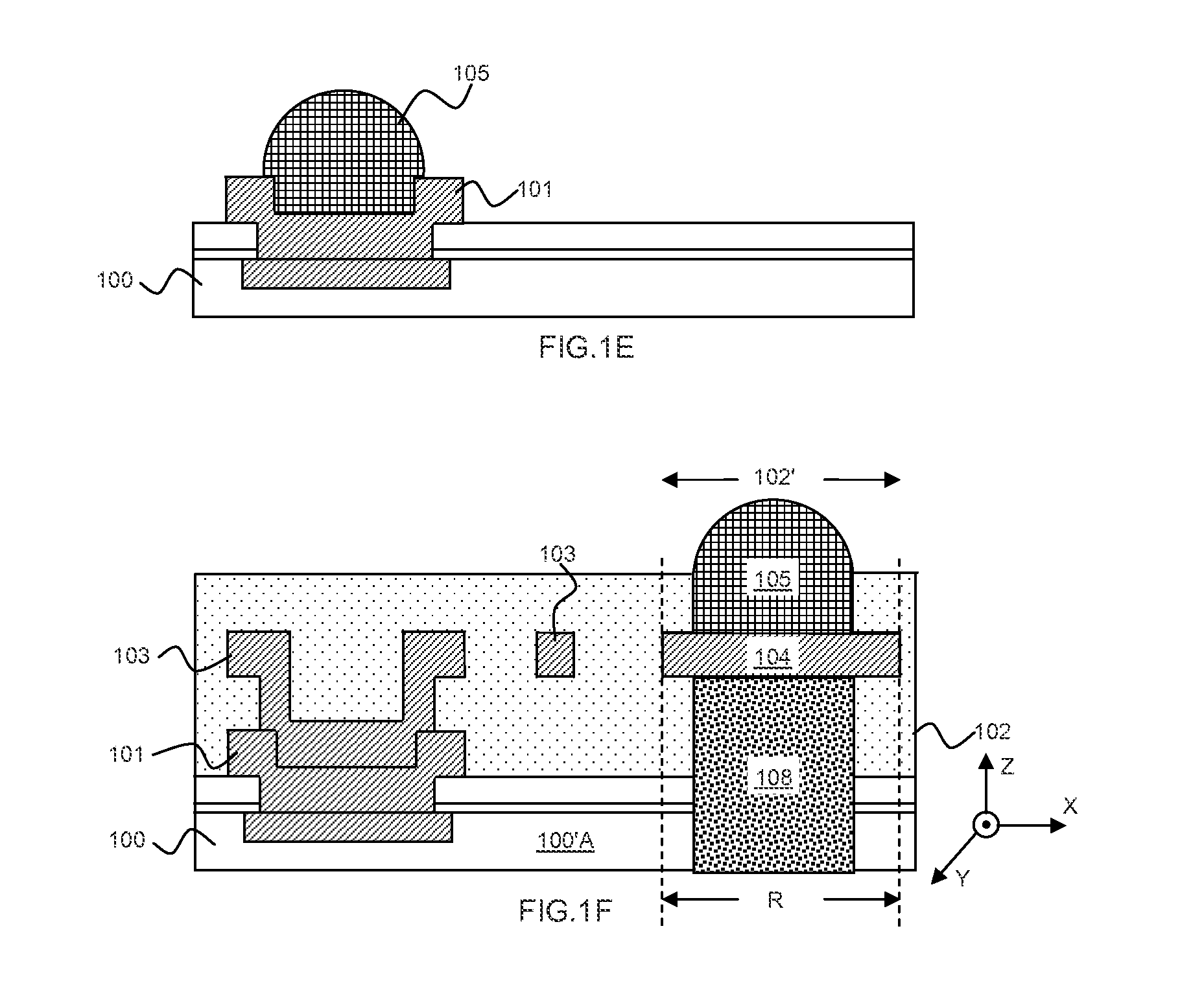
[0023]Referring to FIG. 1A, which shows a top view of a semiconductor chip 100, a plurality of bonding pads 101 connected with the circuits in the chip 100 are formed around the edges at the top side of the chip 100. Usually, the bonding pads 101 are aluminum pads used for electrically connecting to the outside devices. For example, bonding wire is directly formed on the bonding pads or solder bump is formed on the under-bump metallurgy (UBM) layers, such as Ti, Cu or Ni layer, which are deposited on the bonding pads for connecting to the peripheral devices. The bonding pads can be the I / O pad or Power or Ground interface of the circuit in the semiconductor chip 100. FIG. 1B is a cross sectional view that illustrates the bonding pads 101 formed on the edge at the top surface of the semiconductor chip 100.

[0024]Referring to FIG. 1C, by utilizing RDL (Redistribution Layer) technique, the bonding pads formed around the edges at the top surface of the semiconductor chip 100 can be redis...


PUM


Abstract

The present invention relates to a package for semiconductor device and the fabrication method for integrally encapsulating a whole semiconductor chip within a molding compound. In the semicondcutor device package, bonding pads distributed on the top of the chip are redistributed into an array of redistributed bonding pads located in an dielectric layer by utilizing the redistribution technique. The electrodes or signal terminals on the top of the semiconductor chip are connected to an electrode metal segment on the bottom of the chip by conductive materials filled in through holes formed in a silicon substrate of a semiconductor wafer. Furthermore, the top molding portion and the bottom molding portion seal the semiconductor chip completely, thus providing optimum mechanical and electrical protections.

Description

FIELD OF THE INVENTION[0001]The present invention relates to a package for semiconductor device and the fabrication method thereof, and more particularly to a package structure and the Wafer Level Chip Scale Packaging (WLCSP) method for thin semiconductor chips.BACKGROUND OF THE INVENTION[0002]In the advanced chip packaging methods, the WLCSP (Wafer Level Chip Scale Packaging) technique is a technique in which packaging and tests are performed on a semiconductor wafer and then the wafer is molded and singulated into individual IC packages. The IC package size after packaging is almost the same as the original size of the bare die. The package has good heat dissipation and electrical properties.[0003]Usually, the thickness of the semiconductor chip is reduced to a certain value based on the requirement of substrate resistance reduction or chip size reduction. However, the thinner the chip is, the more easily it cracks. Therefore, any shape modification of the semiconductor chip shoul...

Claims


Application Information

Patent Timeline
IPC IPC(8): H01L23/498H01L21/78
CPCH01L21/76898H01L23/481H01L2924/00014H01L2924/1306H01L2224/0401H01L2224/05554H01L2224/02166H01L2224/131H01L2221/68377H01L2221/68359H01L2221/6834H01L21/6836H01L24/13H01L24/11H01L24/05H01L2924/13091H01L2224/05548H01L2224/05571H01L2224/13009H01L2224/13022H01L2224/13024H01L2224/94H01L2224/1184H01L23/3114H01L23/3135H01L21/561H01L24/03H01L2224/03H01L2224/11H01L2924/00012H01L2924/014H01L2924/00H01L2224/05552H01L2924/12042H01L2924/181
Inventor XUE, YAN XUNHUANG, PINGHO, YUEH-SEYILMAZ, HAMZALU, JUNLU, MING-CHEN
Owner ALPHA & OMEGA SEMICON INC
Why Eureka
Try Eureka