Output driving circuit and transistor output circuit

a driving circuit and output circuit technology, applied in oscillator generators, pulse techniques, instruments, etc., can solve the problems of increasing current consumption, increasing current consumption, and high frequency, and achieve stable operation, low current consumption, and stable operation

Inactive Publication Date: 2013-02-14
SAMSUNG ELECTRO MECHANICS CO LTD
View PDF5 Cites 14 Cited by
  • Summary
  • Abstract
  • Description
  • Claims
  • Application Information

AI Technical Summary

Benefits of technology

[0014]Further, it is another object of the present invention to provide an output driving circuit and a transistor output circuit that

Problems solved by technology

The conventional technology of FIG. 6 is disadvantageous to a relatively high frequency since a gate-source capacitance of the output transistor T1 is charged through the resistor and discharged through a current source and increases current consumption since a current I continuously flows thr

Method used


Image

  • Output driving circuit and transistor output circuit
  • Output driving circuit and transistor output circuit
  • Output driving circuit and transistor output circuit

Examples


first embodiment

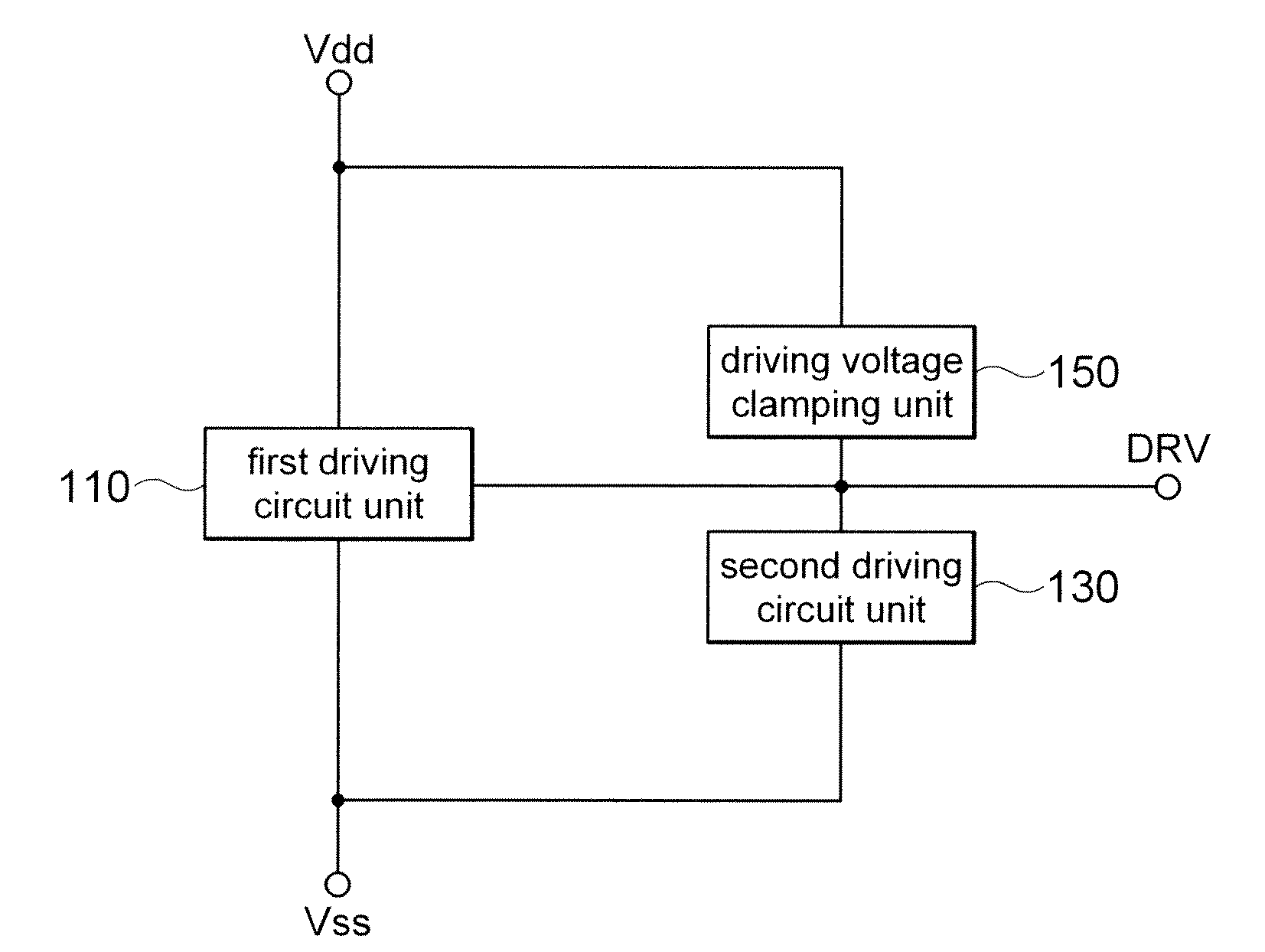
[0039]First, an output driving circuit in accordance with a first embodiment will be described in detail with reference to the drawings.

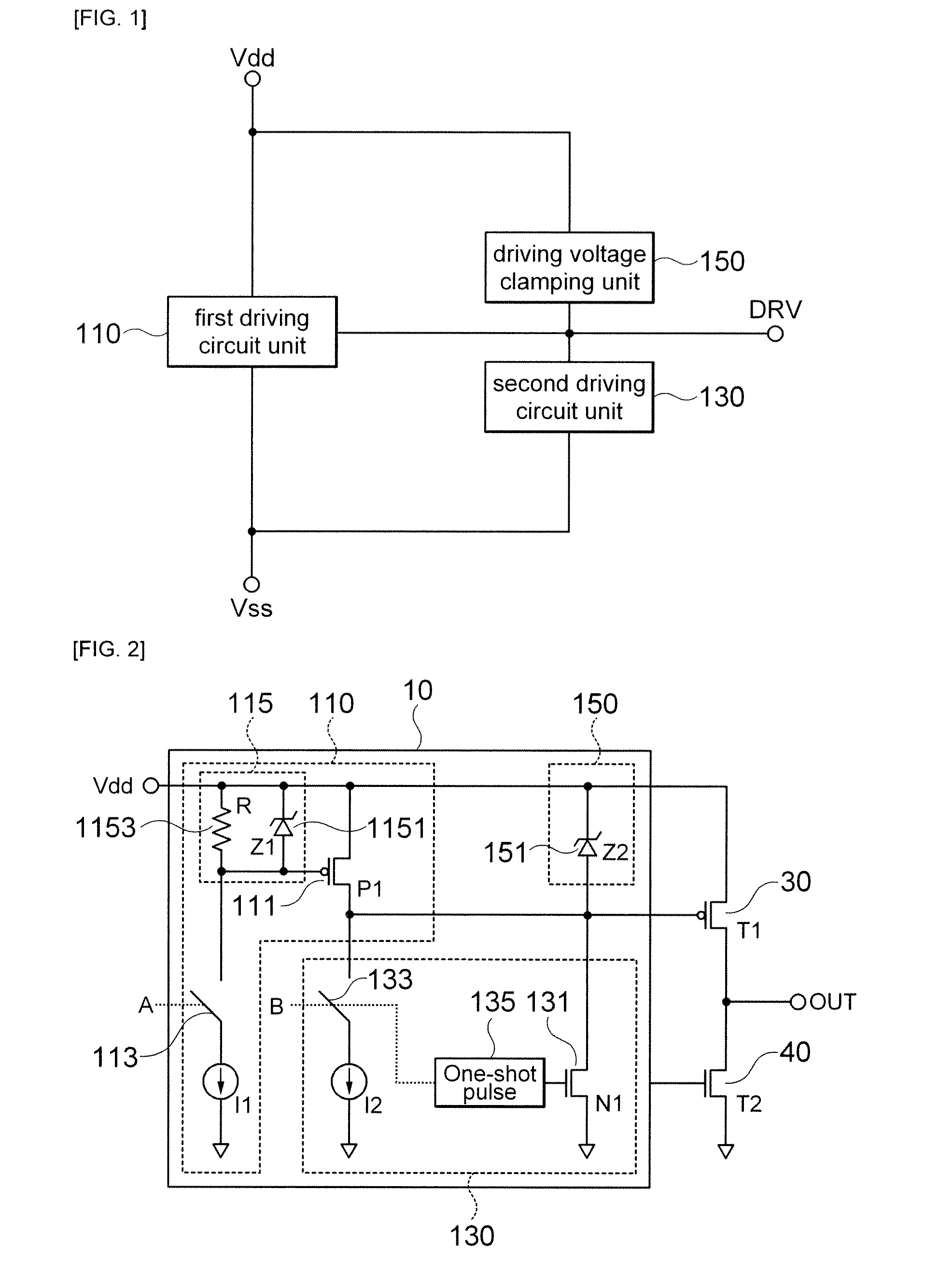
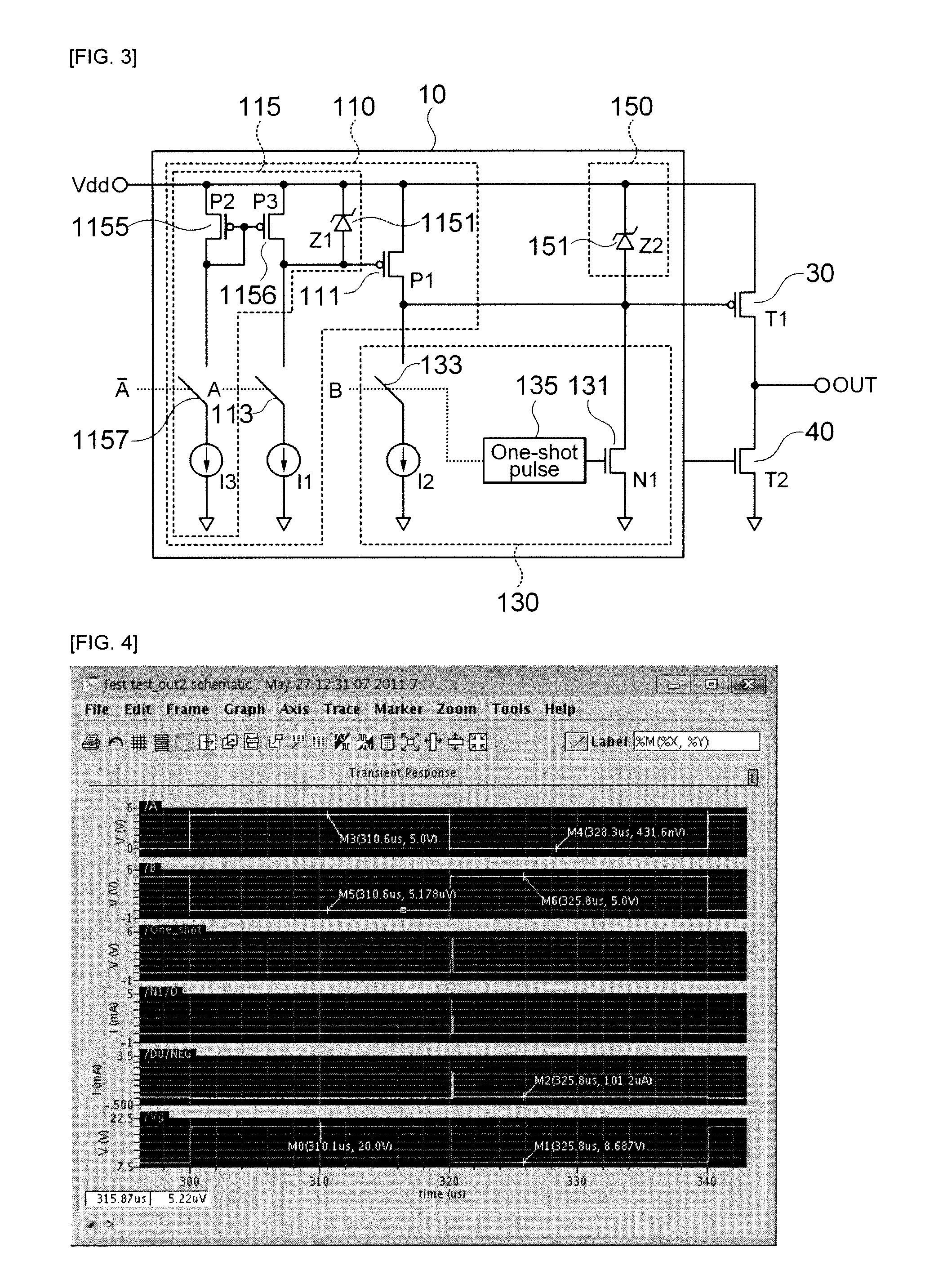
[0040]FIG. 1 is a block diagram roughly showing an output driving circuit in accordance with an embodiment of the present invention. FIG. 2 is a circuit diagram showing a transistor output circuit including the output driving circuit in accordance with an embodiment of the present invention. FIG. 3 is a circuit diagram showing a transistor output circuit including an output driving circuit in accordance with another embodiment of the present invention. FIG. 4 is a graphic showing a simulation result of the output driving circuit in accordance with an embodiment of the present invention. FIG. 5 is a graphic showing an effect of a one-shot pulse in accordance with an embodiment of the present invention.

[0041]An output driving circuit in accordance with an embodiment of the present invention will be described with reference to FIGS. 1, 2, or / and 3. Ref...

second embodiment

[0067]Next, a transistor output circuit in accordance with the present invention will be described with reference to the drawings. FIG. 2 is a circuit diagram showing a transistor output circuit in accordance with an embodiment of the present invention, and FIG. 3 is a circuit diagram showing a transistor output circuit including an output driving circuit in accordance with another embodiment of the present invention.

[0068]Referring to FIGS. 2 or / and 3, a transistor output circuit in accordance with this embodiment includes a p-channel output transistor 30, an n-channel output transistor 40, and an output driving circuit 10. In FIGS. 2 or / and 3, connection of the output driving circuit 10 and the p-channel and n-channel output transistors 30 and 40 shows that the output driving circuit 10 complementarily drives the p-channel and n-channel output transistors 30 and 40. At this time, the output driving circuit 10 is an output driving circuit 10 in accordance with the foregoing first e...


PUM


Abstract

The present invention relates to an output driving circuit and a transistor output circuit. In accordance with an embodiment of the present invention, an output driving circuit including: a first driving circuit unit driven according to on operation of a first switch to supply high voltage power source to a gate of an output transistor; a second driving circuit unit driven by a one-shot pulse generated according to on operation of a second switch, which operates complementarily with the first switch, to discharge a gate-source capacitance of the output transistor; and an output driving voltage clamping unit disposed between a high voltage power source terminal and the gate of the output transistor in parallel with the first driving circuit unit to maintain a gate potential of the output transistor discharged according to the on operation of the second switch is provided.

Description

CROSS-REFERENCE TO RELATED APPLICATIONS[0001]Claim and incorporate by reference domestic priority application and foreign priority application as follows:[0002]“CROSS REFERENCE TO RELATED APPLICATION[0003]This application claims the benefit under 35 U.S.C. Section 119 of Korean Patent Application Serial No. 10-2011-0080760, entitled filed Aug. 12, 2011, which is hereby incorporated by reference in its entirety into this application.”BACKGROUND OF THE INVENTION[0004]1. Field of the Invention[0005]The present invention relates to an output driving circuit and a transistor output circuit, and more particularly, to an output driving circuit and a transistor output circuit that are capable of stably operating when a high voltage lower than a source-drain breakdown voltage but higher than a gate-source breakdown voltage is applied to a gate of an output transistor.[0006]2. Description of the Related Art[0007]A p-channel transistor, for example, an operating voltage of a p-channel LDMOS is...

Claims


Application Information

Patent Timeline
IPC IPC(8): H03K3/00
CPCH03K17/164G05F3/02
Inventor HEO, CHANG JAE
Owner SAMSUNG ELECTRO MECHANICS CO LTD
Why Eureka
Try Eureka