Thermoelectric device

a technology of thermoelectric devices and thermoelectric devices, which is applied in the manufacture/treatment of thermoelectric devices, thermoelectric devices, and thermoelectric device details. it can solve the problems of difficult processing and manipulation, and achieve the effects of low expected cost, low cost and cheap materials

Inactive Publication Date: 2013-02-21
SONY CORP
View PDF21 Cites 16 Cited by
  • Summary
  • Abstract
  • Description
  • Claims
  • Application Information

AI Technical Summary

Benefits of technology

[0036]The present invention has the advantage that the thermogenerators in accordance with the invention are simple and easy to produce. The expected costs are low, because of cheap materials and amenable production steps being used. Toxic or harmful materials, such as heavy metals, can be avoided altogether. The process can be scaled up, and flexible substrates can be used, thereby widening the possible applications enormously.

Problems solved by technology

They are expensive, belong to the group of heavy metals, with all the environmental problems associated therewith, are rigid and brittle, and are therefore somewhat difficult to process and to manipulate.

Method used


Image

  • Thermoelectric device
  • Thermoelectric device
  • Thermoelectric device

Examples


example 1

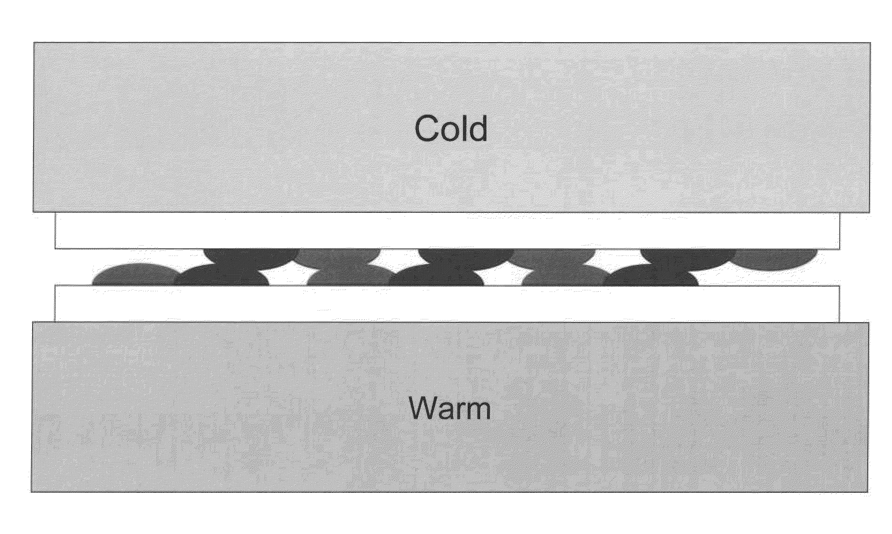
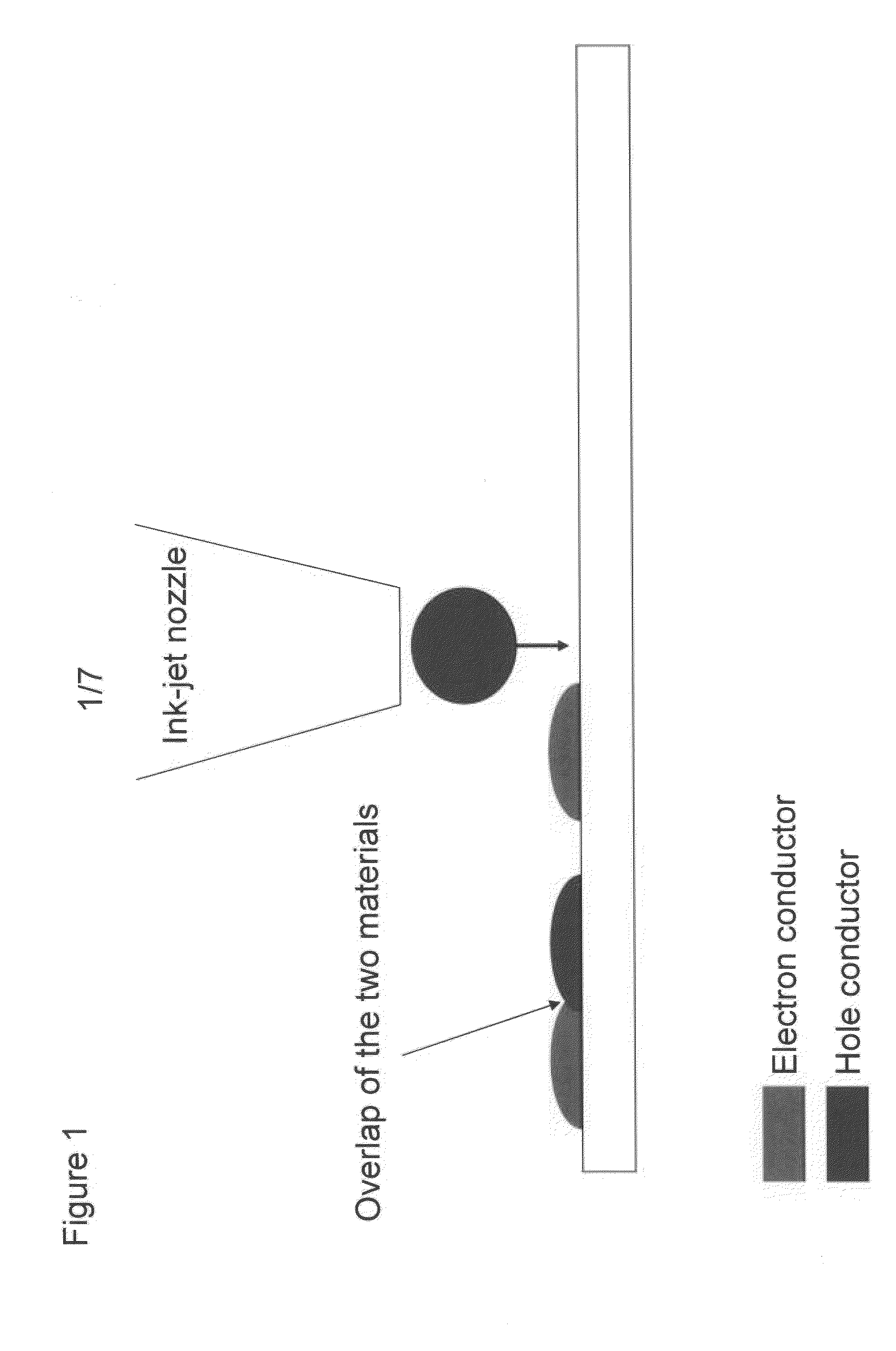
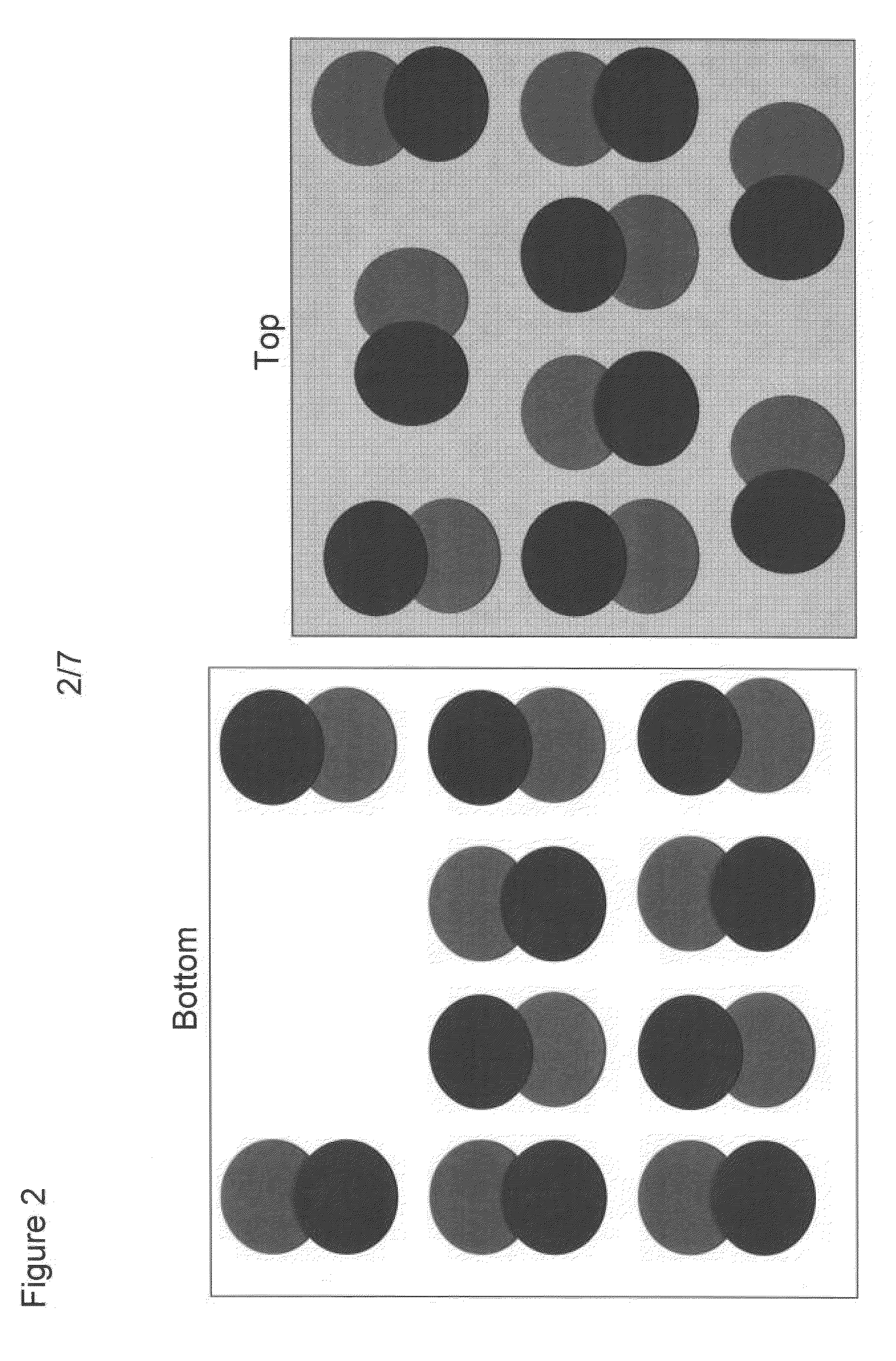
[0047]An embodiment of the process is depicted in FIGS. 1 to 5. Two substrates need to be coated with hole and electron conducting organic material (for example using a solution-based ink-jet printer as depicted in FIG. 1, but any other printing technique or thermal evaporation can be used as well). The two substrates need to have a complementary design, for example the ones depicted in FIG. 2. FIG. 3 illustrates how the two complementary top and bottom substrates are brought together to build a single device. The same is illustrated in FIG. 4 for the design of FIG. 2 after the two halfs have been brought together (top view). The two electron and hole conducting regions on the bottom substrate that protrude out beyond the top substrate are used as contacts to either collect the generated electrical voltage (thermogenerator) or to apply the external voltage (Peltier element). FIG. 5 shows the final usage of the device. It either acts as a thermogenerator, i.e. it produces electrical ...

example 2

[0048]In a prototype-production, a thermogenerator was printed using a nano-plotter and a commercial accessory, “Delo-Dot”, which is a microdispensing valve (www.venso.se / pdf / delo / delodot.pdf) for printing highly viscous liquids. The exemplary P-type semiconducting material and N-type semiconducting material are shown in FIG. 6. The dimensions to be used for the prototype thermogenerator were as follows:

[0049]Dimensions:[0050]Squares: 3×3 mm (16×16 dots, 0.2 mm grid)[0051]Rectangles: 5×3mm (26×16 dots, 0.2 mm grid)[0052]Gap: 1 mm

[0053]Settings of the Delo-Dot:[0054]100V[0055]40 μs[0056]100 Hz[0057]0.5 bar[0058]1 droplet per point

[0059]Substrate: HP LaserJet transparency foil (roughly 5×5 cm)

[0060]Substrate cleaning: 15 min in UVO-cleaner

[0061]Pressed the two substrates together on a hotplate at 120° C. for 15 min using pressure of approximately 800N / m2

[0062]The resultant thermogenerator that was thus produced can be seen in FIG. 7.

example 3

[0063]In the following some suitable materials are shown that can be used as organic semiconducting materials of the n-type and p-type. Typically, for these materials organic polymers can be used, which may or may not be doped using electron donors, e.g. phosphorus, to give n-type conduction, or using electron acceptors, e.g. boron, to give p-type conduction.

[0064]Suitable polymers include for example poly(3-hexylthiophene) (P3HT), polyaniline, poly(phenylene vinylene)-disperse red 1 (PPV-DR1), polysiloxane carbazole (PSX-Cz), polypyrrole, poly(o-anthranilic acid) (PARA), poly(aniline-co-o-anthranilic acid) (PANI-PARA) and poly(3,4-ethylenedioxythiophene) (PEDOT). The structural formulas of some the above mentioned polymers are shown below:

[0065]Mixtures of polymers (e.g. PEDOT:PSS or PEDOT:Tos) or copolymers can also be used.

[0066]In order to induce charges into the polymer these materials can be doped, using for example electron donors (e.g phosphorous→n-type conduction) or electr...


PUM

PropertyMeasurementUnit
areaaaaaaaaaaa
pressureaaaaaaaaaa
semiconductingaaaaaaaaaa

Abstract

The present invention relates to a thermoelectric device, in particular an all-organic thermoelectric device, and to an array of such thermoelectric devices. Furthermore, the present invention relates to a method of manufacturing a thermoelectric device, in particular an all-organic thermoelectric device. Moreover, the present invention relates to uses of the thermoelectric device and/or the array in accordance with the present invention.

Description

CROSS-REFERENCE TO RELATED APPLICATIONS[0001]The present application claims priority to and incorporates by reference the entire contents of European Patent Application No. 11 005 765.0 filed on Jul. 14, 2011.BACKGROUND OF THE INVENTION[0002]The present invention relates to a thermoelectric device, in particular an all-organic thermoelectric device, and to an array of such thermoelectric devices. Furthermore, the present invention relates to a method of manufacturing a thermoelectric device, in particular an all-organic thermoelectric device. Moreover, the present invention relates to uses of the thermoelectric device and / or the array in accordance with the present invention.[0003]State of the art thermoelectric devices, i.e. thermogenerators and Peltier elements, are made of inorganic semiconductors, mostly based on bismuth and tellurium. While these materials have large advantages as superior efficiency or high output voltages, they also show several disadvantages. They are expens...

Claims


Application Information

Patent Timeline
Patent Type & Authority Applications(United States)
IPC IPC(8): H01L35/24H01L35/02H01L21/98H01L35/34
CPCH01L35/24H01L35/34H01L51/0005H01L51/0583H01L51/0039H01L51/0059H01L51/0036H10N10/856H10N10/01H10K71/135H10K85/113H10K85/115H10K85/631H10K10/26
Inventor WIRTZ, RENEROSSELLI, SILVIANELLES, GABRIELE
Owner SONY CORP
Why Eureka
Try Eureka