Method of Manufacturing a Metallized Ceramic Substrate

Inactive Publication Date: 2013-02-28
VIKING TECH L C
View PDF1 Cites 1 Cited by
  • Summary
  • Abstract
  • Description
  • Claims
  • Application Information

AI Technical Summary

Benefits of technology

[0019]From the context mentioned above, it can be known that notch, void or groove can be easily and reliably formed on the boundary of the metal layer of the metallized ceramic substrate due to the dexterous design of the openings in width of the resist in this application. Besides, this application can further remove part of the metal layer by brushing, grinding of mounted points, sandblasting or electrical discharge machining so tha

Problems solved by technology

This conchoidal fracture arises from the mismatch of thermal expansion generated by internal stress during the thermal shock fracturing of the ceramic layer under the copper layer rather than the fracturing at the interface between the ceramic layer and copper layer.
However, the opening aperture of the copper layer, lateral profile and etching depth from this kind of etching method can not be easily controlled, and the final etching structure is not exactly identical to the original design figure as a result, causing that the reduction of the stress is not so large as expected.
For example, if the etching time i

Method used


Image

  • Method of Manufacturing a Metallized Ceramic Substrate
  • Method of Manufacturing a Metallized Ceramic Substrate
  • Method of Manufacturing a Metallized Ceramic Substrate

Examples


first embodiment

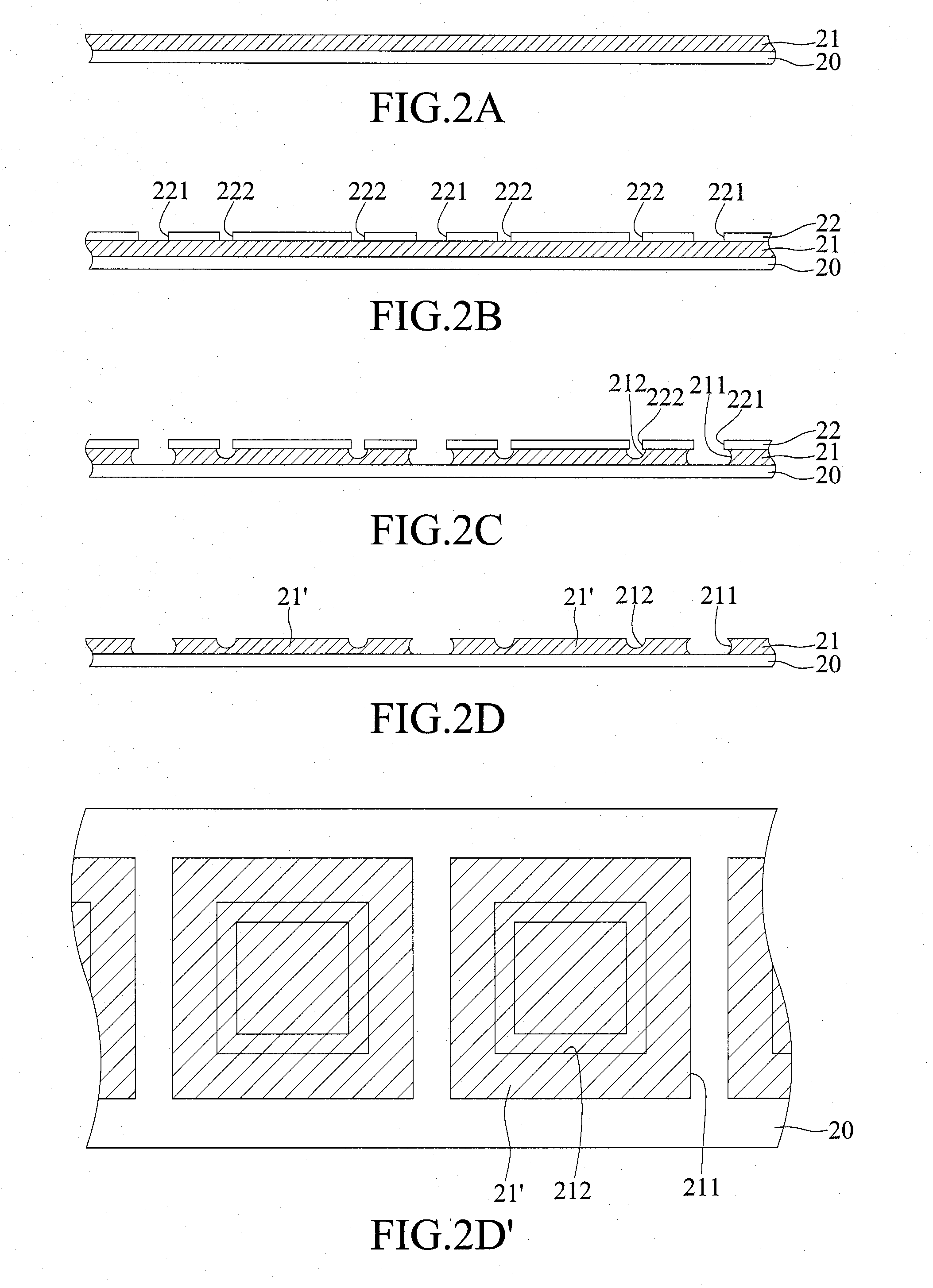
[0028]Please refer to FIGS. 2A to 2D, which are cross-sectional diagrams illustrating a method of manufacturing a metallized ceramic substrate of a first embodiment according to the present invention, wherein FIG. 2D′ is the top view of FIG. 2D.

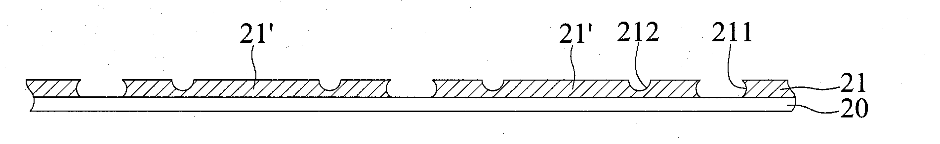
[0029]As FIG. 2A illustrates, a ceramic substrate 20 is provided, and a metal layer 21 is formed on the ceramic substrate 20, wherein the metal layer 21 may be made of copper or aluminum.

[0030]As FIG. 2B illustrates, a resist 22 is formed on the metal layer 21, and has first patterned resist openings 221 and second patterned resist openings 222 for the metal layer 21 to be exposed therefrom. The width of the first patterned resist openings 221 is greater than 1.2 times of the thickness of the metal layer 21, and the width of the second patterned resist openings 222 is less than 1.2 times of the thickness of the metal layer 21.

[0031]As FIG. 2C illustrates, a wet-etching process is conducted. Because the wet-etching process is an isotropically ...

second embodiment

[0036]Please refer to FIGS. 3A to 3B, which are cross-sectional diagrams of a method of manufacturing a metallized ceramic substrate in a second embodiment according to the present invention.

[0037]As FIGS. 3A to 3B illustrate, subsequent to the processes performed in FIG. 2D, brushing wheels 30 brush the metal layer 21. A sand belt (not shown) may be disposed on the surface of the brushing wheels 30. A stress concentration effect may occur at a top periphery of the patterned metal layer openings 211 and the patterned metal layer dents 212 when the brushing wheels 30 are in contact with the metal layer 21. As a result, the metal layer 21 has its edge more easily brushed and removed than its surface, and the top periphery of the patterned metal layer openings 211 and the patterned metal layer dents 212 are in a curved shape, which effectively alleviating the internal stress between the metal layer 21 and the ceramic substrate 20.

[0038]In the first embodiment, the brushing wheels 30 br...

third embodiment

[0040]Please refer to FIGS. 4A and 4B, which are cross-sectional diagrams of a method of manufacturing a metallized ceramic substrate of a third embodiment according to the present invention.

[0041]As FIGS. 4A to 4B illustrate, subsequent to the processes performed in FIG. 2D, mounted points 40 brushes and removes the metal layer 21 at the top periphery of the patterned metal layer openings 211. The head 401 of the mounted points 40 may be in the conical or cylindrical shapes such that the top periphery of the patterned metal layer openings 211 are in the shape of a inclined plane or a step, which also have reduced internal stress between the metal layer 21 and the ceramic substrate 20.

[0042]In the method according to the present invention, the formation of the patterned metal layer dents is optional. Accordingly, only the patterned metal layer openings are formed by performing the wet-etching process on the ceramic substrate, and the metal layer at the top periphery of the patterned...


PUM

PropertyMeasurementUnit
Thicknessaaaaaaaaaa
Shapeaaaaaaaaaa
Stress optical coefficientaaaaaaaaaa

Abstract

A method of manufacturing a metallized ceramic substrate includes forming a metal layer on a ceramic substrate, and forming on the metal layer a resist having a first patterned resist opening and a second patterned resist opening for the metal layer to be exposed therefrom. A first width of the first patterned resist opening is greater than the thickness of the metal layer, and a second width of the second patterned resist opening is less than the thickness of the metal layer. A wet-etching process is conducted, to form in the first patterned resist opening a patterned metal layer opening and form in the second patterned resist opening a patterned metal layer dent. Therefore, an internal stress between the metal layer and the ceramic substrate is reduced, and the yield rate and reliability of the metallized ceramic substrate is increased.

Description

FIELD OF THE INVENTION[0001]This invention relates to methods of manufacturing a metallized ceramic substrate, and, more particularly, to a method of manufacturing a metallized ceramic substrate that has a reduced internal stress.DESCRIPTION OF RELATED ART[0002]Along with the rapid development of electronic industry, electronic products are indispensable for modern people. In general, an electronic product includes a metallized ceramic substrate such as a ceramic plate covered with copper. The ceramic plate covered with copper is generally formed by a ceramic layer sintered with a metal layer such as a copper layer by a direct bonded copper (DBC) technique at a high temperature. After sintered, the ceramic layer and the copper layer have a strong bonding force therebetween and the ceramic plate covered with copper is thus highly reliable. However, there is a fracture mode called conchoidal fracture which is an irregular and a fracture mode along a non-lattice plane between the ceram...

Claims


Application Information

Patent Timeline
IPC IPC(8): C23F1/02
CPCH01L21/4807Y10T428/24926C23F1/02H01L23/15H01L2924/0002Y10T428/31678
Inventor WEI, SHIH-LONGHSIAO, SHEN-LIHO, CHIEN-HUNG
Owner VIKING TECH L C
Why Eureka
Try Eureka