Data read circuit, a non-volatile memory device having the same, and a method of reading data from the non-volatile memory device

Active Publication Date: 2013-02-28
SAMSUNG ELECTRONICS CO LTD
View PDF4 Cites 51 Cited by
  • Summary
  • Abstract
  • Description
  • Claims
  • Application Information

AI Technical Summary

Benefits of technology

[0008]The inventive concept provides a data read circuit capable of improving the performance of a semiconductor memory device by guaranteeing data reliability in view of multiple factors that typically hav

Problems solved by technology

However, due to a number of factors such as process variations that occur when the semiconductor memory device is fabricated or a variation in signals prov

Method used


Image

  • Data read circuit, a non-volatile memory device having the same, and a method of reading data from the non-volatile memory device
  • Data read circuit, a non-volatile memory device having the same, and a method of reading data from the non-volatile memory device
  • Data read circuit, a non-volatile memory device having the same, and a method of reading data from the non-volatile memory device

Examples


Example

[0065]Hereinafter, exemplary embodiments of the inventive concept will be described in detail with reference to the accompanying drawings. Throughout the drawings and specification, like reference numerals may refer to like elements.

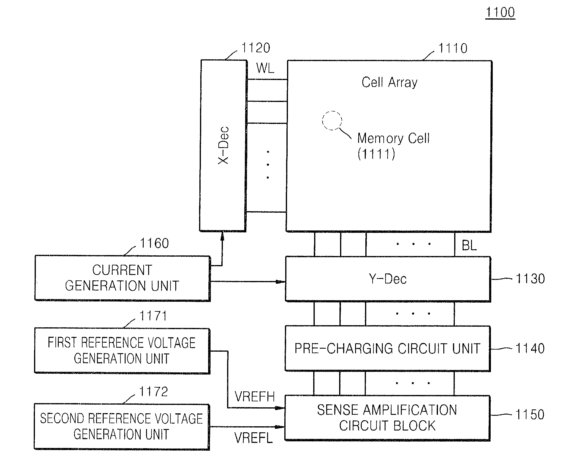
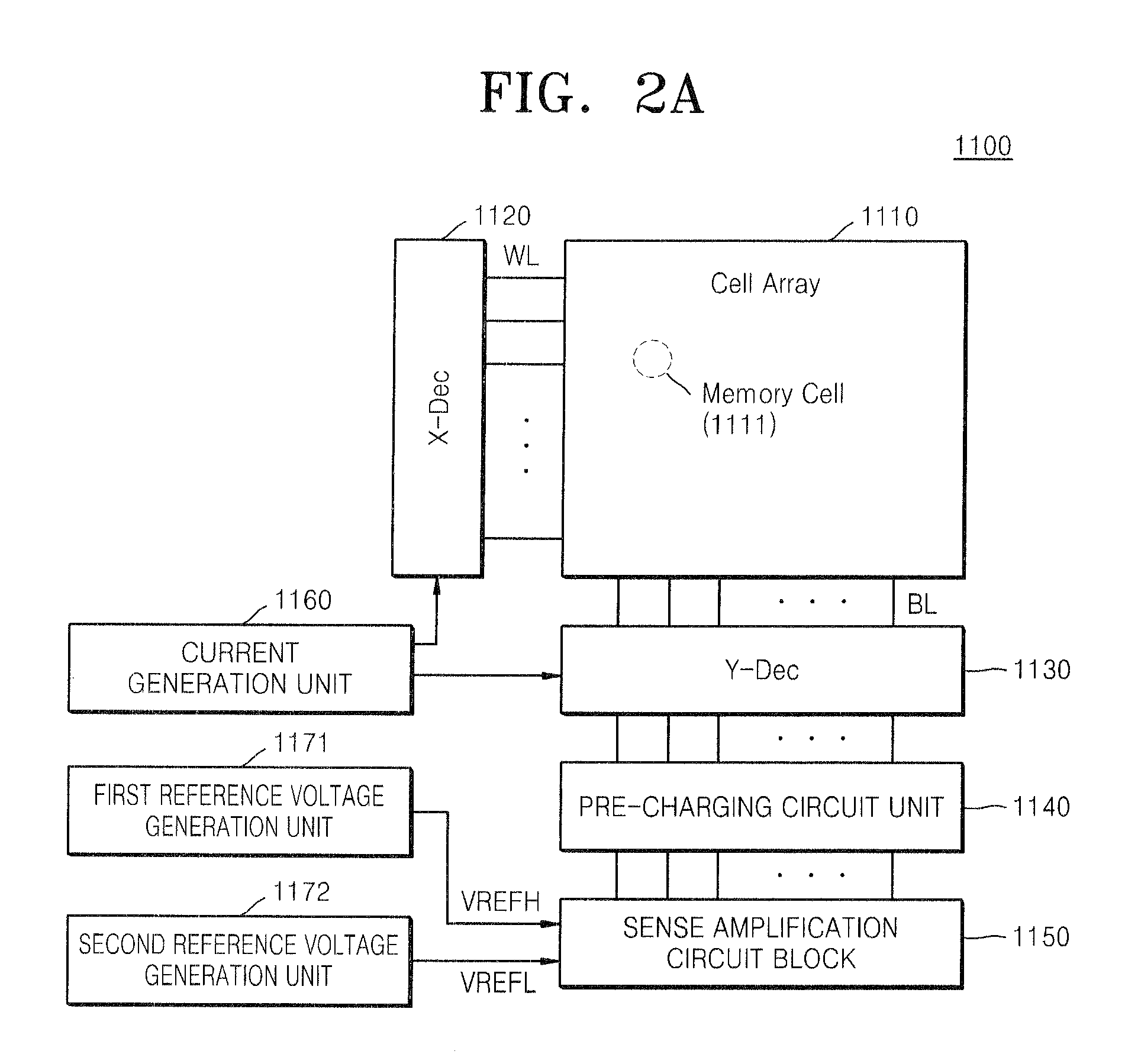
[0066]Examples of non-volatile memory devices may include a Phase Change Random Access Memory (PRAM), a Resistive Random Access Memory (RRAM), a Magnetic Random Access Memory (MRAM), and a Ferroelectric Random Access Memory (FRAM). The non-volatile memory devices such as the PRAM, the RRAM, and the MRAM may have low-cost and high-capacity features of a Dynamic Random Access Memory (DRAM), an operating speed of a Static Random Access Memory (SRAM), and non-volatility of a flash memory. For example, a read access time of a Spin Torque Transfer (STT)-MRAM, which is a type of MRAM, has been reduced to 10 ns or less.

[0067]In general, a non-volatile memory device includes a read circuit for reading data of a memory cell, and the read circuit includes a sense a...


PUM


Abstract

A non-volatile memory device including a cell array, which includes a plurality of memory cells, and a sense amplification circuit. The sense amplification circuit is configured to receive a data voltage of a memory cell, a first reference voltage and a second reference voltage during a data read operation of the memory cell, generate differential output signals based on a voltage level difference between the data voltage and the first and second reference voltages, and output the differential output signals as data read from the memory cell.

Description

CROSS-REFERENCE TO RELATED APPLICATIONS[0001]This application claims priority under 35 U.S.C. §119 to Korean Patent Application No. 10-2011-0085146, filed on Aug. 25, 2011, in the Korean Intellectual Property Office and Korean Patent Application No. 10-2011-0110719, filed on Oct. 27, 2011, in the Korean Intellectual Property Office, the disclosures of which are incorporated by reference herein in their entireties.BACKGROUND[0002]1. Technical Field[0003]The inventive concept relates to a data read circuit, and more particularly, to a data read circuit for performing a data read operation by using a plurality of reference voltages, a non-volatile memory device including the data read circuit, and a method of reading data from the non-volatile memory device.[0004]2. Discussion of the Related Art[0005]Semiconductor memory is an electronic data storage device, implemented on a semiconductor-based integrated circuit. Examples of semiconductor memory devices may include volatile memory dev...

Claims


Application Information

Patent Timeline
IPC IPC(8): G11C5/14G11C11/00G11C11/16G11C11/22
CPCG11C11/1673G11C13/0004G11C13/0023G11C13/0033G11C13/004G11C13/0061G11C7/14G11C2013/0054G11C11/5678G11C7/062G11C7/067G11C7/08G11C2013/0042G11C11/1693
Inventor KIM, CHAN-KYUNGHWANG, HONG-SUNPARK, CHUL-WOOKANG, SANG-BEOMOH, HYUNG-ROK
Owner SAMSUNG ELECTRONICS CO LTD
Why Eureka
Try Eureka