Group iii nitride semiconductor laser device

a semiconductor laser and nitride technology, applied in semiconductor lasers, laser details, electrical devices, etc., can solve the problems of unsatisfactory crystal quality of the layer to be grown (p-type cladding layer), inability to apply high temperature cleaning, current loss thereat, etc., to increase the threshold current density increase the drive voltage of the semiconductor laser device.

Inactive Publication Date: 2013-02-28
SUMITOMO ELECTRIC IND LTD
View PDF4 Cites 57 Cited by
  • Summary
  • Abstract
  • Description
  • Claims
  • Application Information

AI Technical Summary

Benefits of technology

[0008]In the fabrication of the group-III nitride semiconductor laser device having the structure as described above, an opening is formed by, for example, etching the current confinement layer. The inventors' findings indicate that impurities such as oxygen and silicon, i.e., n-type dopant, are piled up on a semiconductor surface exposed in the opening of the current confinement layer, (i.e., the re-growth surface on which the p-type cladding layer is to be grown). When a semiconductor layer is re-grown by CVD which uses organic metal materials, the exposed surface is usually cleaned with H2 or NH3 at a temperature of 1000 degrees Celsius or higher. The cleaning preferably can remove the above impurities. But, such a high temperature cleaning of the semiconductor structure including the current confinement layer causes modification of the current confinement layer (for example, crystallization), which results in unsatisfactory crystal quality of the layer to be grown (p-type cladding layer) therein. Such a high temperature cleaning cannot be, therefore, applied as a process prior to the re-growth of the p-type cladding layer. Accordingly, the p-type cladding layer is grown on the exposed surface having n-type residual impurities, so that the n-type impurities therein generate non-radiative recombination at the interface between the p-type cladding layer and the optical guiding layer, resulting in current loss thereat. This current loss increases the threshold current density of the semiconductor laser device. The structure in which another p-type semiconductor layer is provided between the p-type cladding layer and the active layer includes a local pnp-structure, and this local structure may increase the drive voltage of the semiconductor laser device.

Problems solved by technology

But, such a high temperature cleaning of the semiconductor structure including the current confinement layer causes modification of the current confinement layer (for example, crystallization), which results in unsatisfactory crystal quality of the layer to be grown (p-type cladding layer) therein.
Such a high temperature cleaning cannot be, therefore, applied as a process prior to the re-growth of the p-type cladding layer.
Accordingly, the p-type cladding layer is grown on the exposed surface having n-type residual impurities, so that the n-type impurities therein generate non-radiative recombination at the interface between the p-type cladding layer and the optical guiding layer, resulting in current loss thereat.
This current loss increases the threshold current density of the semiconductor laser device.

Method used


Image

  • Group iii nitride semiconductor laser device
  • Group iii nitride semiconductor laser device
  • Group iii nitride semiconductor laser device

Examples


Embodiment Construction

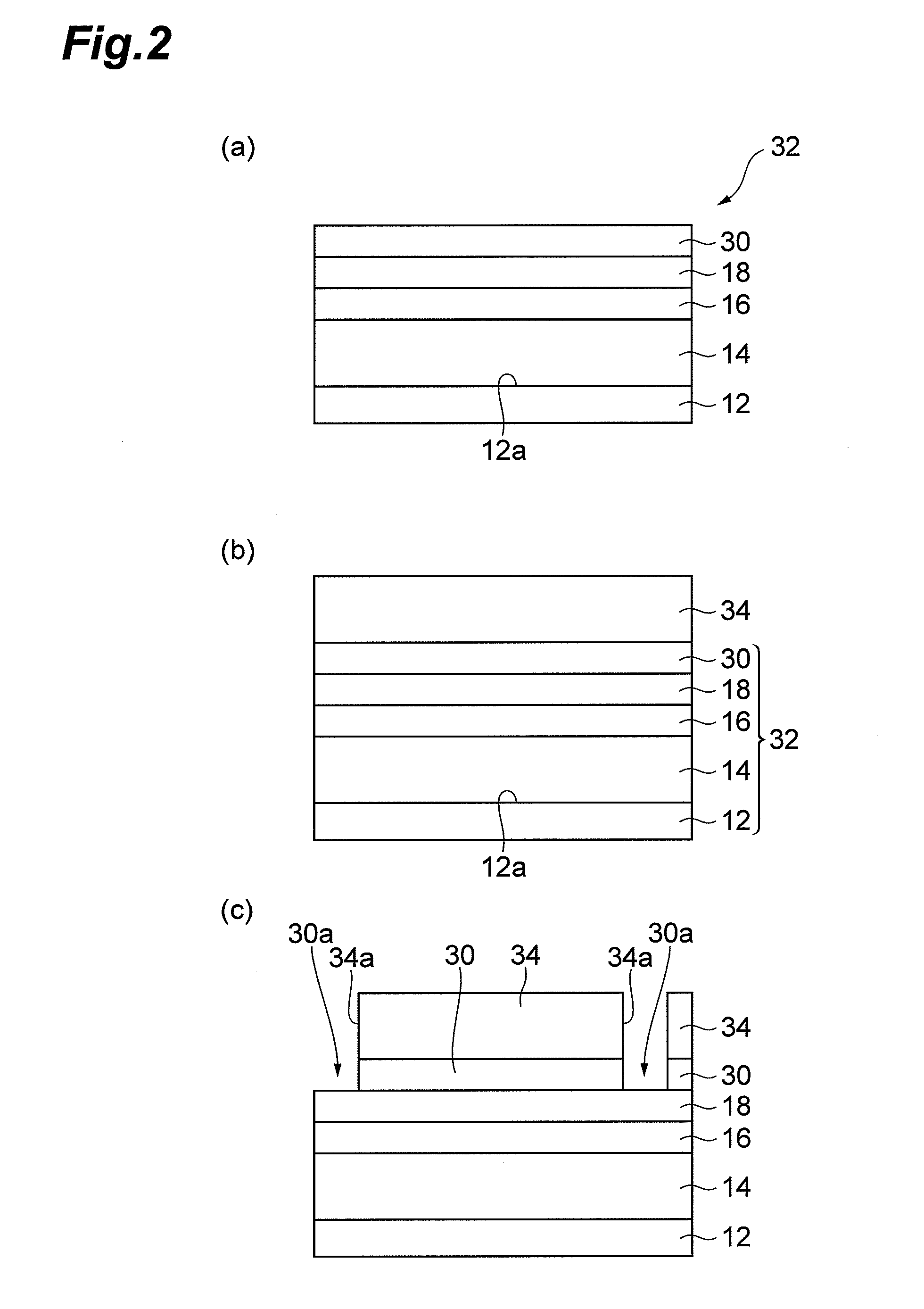
[0026]The teachings of the present invention can be readily apparent from the following detailed descriptions with reference to the accompanying drawings that illustrate typical embodiments. A group-III nitride semiconductor laser device according to an embodiment of the present invention will now be described with reference to the accompanying drawings. If possible, the same reference numerals are assigned to the same components.

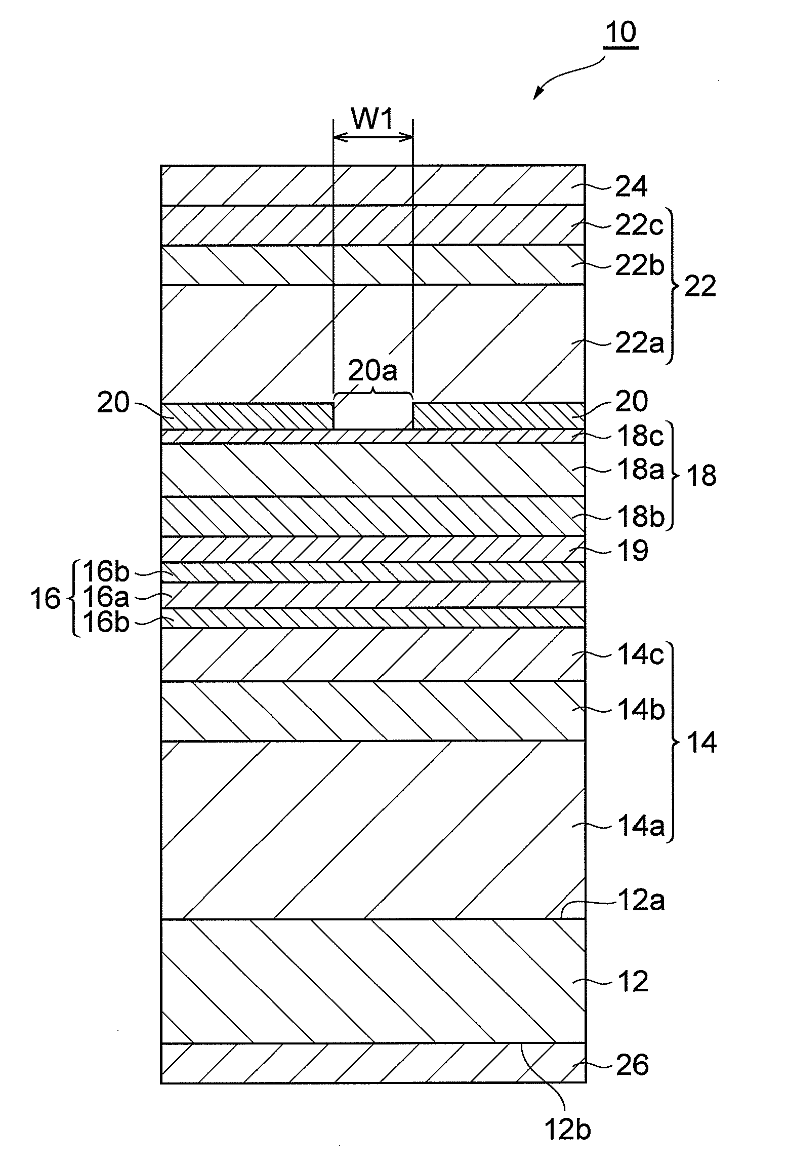
[0027]FIG. 1 is a view illustrating the structure of a semiconductor laser device 10 according to an embodiment of the present invention, and the cross-section or end face thereof is taken along the line vertical to the optical cavity direction. The semiconductor laser device 10 can include a group-III nitride semiconductor laser device which can emit green laser light having an emission wavelength in the range of 500 nm to 540 nm. The semiconductor laser device 10 includes a semiconductor substrate 12 as a support, an n-type semiconductor region 14, an act...


PUM


Abstract

A group-III nitride semiconductor laser device includes an n-type nitride semiconductor region, an active layer provided over the n-type nitride semiconductor region, a first p-type nitride semiconductor region provided over the active layer, a current confinement layer which is provided over the first p-type nitride semiconductor region and has an opening extending in a optical cavity direction, and a second p-type nitride semiconductor region re-grown on the first nitride semiconductor region and the current confinement layer after the formation of the opening of the current confinement layer. The interface between the first p-type nitride semiconductor region and the second p-type nitride semiconductor region includes a semi-polar plane. At least one of the first or second p-type semiconductor regions includes a highly doped p-type semiconductor layer forming an interface with the first and second p-type semiconductor regions and have a p-type impurity level of 1×1020 cm−3 or greater.

Description

BACKGROUND OF THE INVENTION[0001]1. Field of the Invention[0002]This invention relates to a group-III nitride semiconductor laser device.[0003]2. Related Background Art[0004]Patent Literatures 1 to 3 disclose group-III nitride semiconductor laser devices. The group-III nitride semiconductor laser devices disclosed in these patents each include a substrate composed of a group-III nitride semiconductor, an n-type cladding layer of an n-type group-III nitride semiconductor provided on the substrate, an active layer of a group-III nitride semiconductor provided on the n-type cladding layer, a p-type cladding layer of a p-type group-III nitride semiconductor provided on the active layer. An optical guiding layer is provided between the p-type cladding layer and the active layer, and a current confinement layer having an opening for confining current is sandwiched between the optical guiding layer and the p-type cladding layer. A group-III nitride semiconductor laser device having such a ...

Claims


Application Information

Patent Timeline
Patent Type & Authority Applications(United States)
IPC IPC(8): H01S5/323
CPCH01S5/2206H01S5/2231B82Y20/00H01S5/3202H01S5/34333H01S5/3054H01S5/320275
Inventor SUMITOMO, TAKAMICHIUENO, MASAKIYOSHIZUMI, YUSUKEYOSHIDA, TAKAHISAADACHI, MASAHIRO
Owner SUMITOMO ELECTRIC IND LTD
Why Eureka
Try Eureka