Method and system for modifying resist openings using multiple angled ions

a technology of resist openings and ionization, applied in the field of device manufacturing, can solve the problems of inability to print loss of imaging resolution of lithography systems, and inability to achieve accurate openings or holes in resist materials, etc., to achieve improved patterning of substrates, reduce roughness, and improve patter

Active Publication Date: 2013-03-14
VARIAN SEMICON EQUIP ASSOC INC
View PDF13 Cites 7 Cited by
  • Summary
  • Abstract
  • Description
  • Claims
  • Application Information

AI Technical Summary

Benefits of technology

[0012]Embodiments of the present invention are directed to methods and systems for improving patterning a substrate, in particular, by improving patterning in a set of resist features used to pattern an underlying substrate. In an exemplary embodiment, a method of reducing roughness in an opening of a resist material disposed on a substrate, comprises generating a plasma having a plasma sheath and ions therein. The method also includes modifying a shape of a boundary defined between the plasma and the plasma sheath with a plasma sheath modifier so that a portion of the boundary facing the resist material is not parallel to a plane defined by the surface of the substrate. The method also includes providing a first exposure of ions while the substrate is in a first position, the first exposure comprising ions accelerated across the boundary having the modified shape toward the resist material over an angular range with respect to the surface of the substrate.

Problems solved by technology

Although optical lithography is an efficient process with high throughput, the process is not without disadvantages.
One limitation is the inability to print accurate openings or holes within a resist material as the opening size scales smaller.
As the opening dimension scales to smaller dimensions, the lithography system loses imaging resolution.
Because the geometrical shape of a patterned resist feature such as a rough opening is transferred from a resist layer to an underlying permanent layer of a device during patterning of the underlying layer, LWR and LER can limit the ability to form trenches or vias of acceptable quality for small opening dimensions, such as those below about 100 nm in lateral size.
Such variations may lead to non-uniform circuits and ultimately device degradation or failure.
Other known techniques, including shrink assist film for enhanced resolution (SAFIER™), and cross contact double patterning, are complex and involve multiple steps to implement.

Method used


Image

  • Method and system for modifying resist openings using multiple angled ions
  • Method and system for modifying resist openings using multiple angled ions
  • Method and system for modifying resist openings using multiple angled ions

Examples


Embodiment Construction

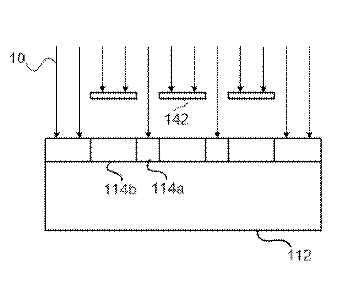
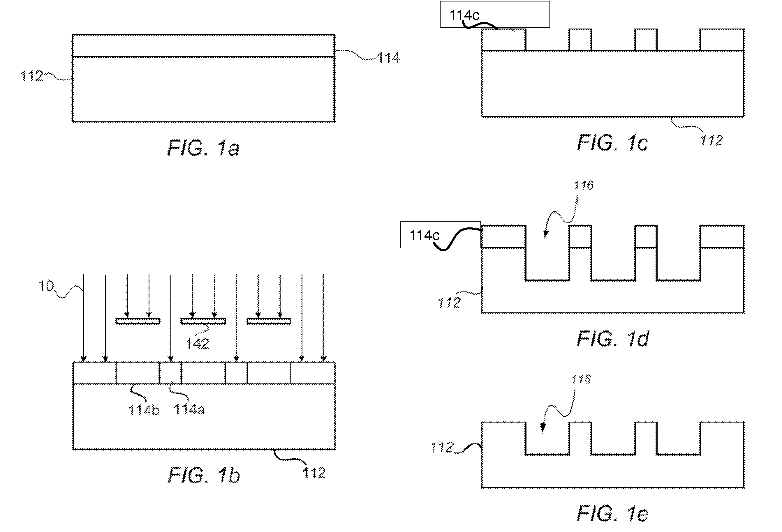
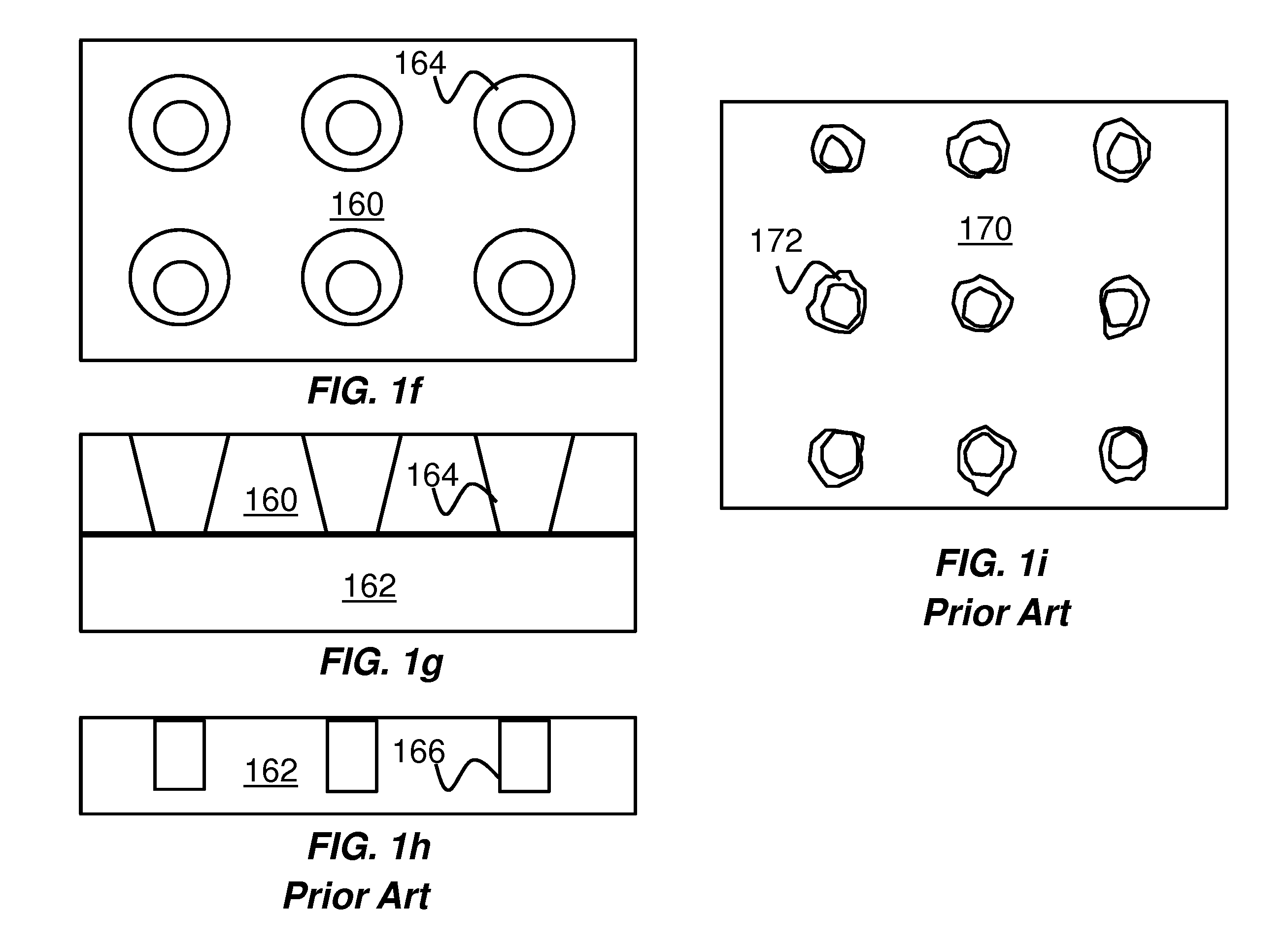
[0029]The present invention will now be described more fully hereinafter with reference to the accompanying drawings, in which preferred embodiments of the invention are shown. This invention, however, may be embodied in many different forms and should not be construed as limited to the embodiments set forth herein. Rather, these embodiments are provided so that this disclosure will be thorough and complete, and will fully convey the scope of the invention to those skilled in the art. In the drawings, like numbers refer to like elements throughout.

[0030]To solve the deficiencies associated with the methods noted above, novel and inventive techniques and systems for patterning a substrate are introduced. In particular, the present disclosure focuses on techniques involving ion implantation processes for improving the quality of resist openings. The processes disclosed herein may be used in conjunction with processes for forming narrow features, including features that are incorporate...


PUM

PropertyMeasurementUnit
twist angleaaaaaaaaaa
anglesaaaaaaaaaa
wavelengthsaaaaaaaaaa

Abstract

A method of reducing roughness in an opening in a surface of a resist material disposed on a substrate, comprises generating a plasma having a plasma sheath and ions therein. The method also includes modifying a shape of a boundary defined between the plasma and the plasma sheath with a plasma sheath modifier so that a portion of the boundary facing the resist material is not parallel to a plane defined by the surface of the substrate. The method also includes providing a first exposure of ions while the substrate is in a first position, the first exposure comprising ions accelerated across the boundary having the modified shape toward the resist material over an angular range with respect to the surface of the substrate.

Description

BACKGROUND OF THE INVENTION[0001]1. Field of the Invention[0002]Embodiments of the invention relate to the field of device manufacturing. More particularly, the present invention relates to a method, system and structure for patterning a substrate and for implanting into a substrate for manufacturing a device.[0003]2. Discussion of Related Art[0004]Optical lithography is often used in manufacturing electronic devices. It is a process by which a substrate is patterned so that circuit may be formed on the substrate according to the pattern. Referring to FIG. 1a-1e, there are shown simplified illustrations of the optical lithographic process. Generally, the substrate 112 is coated with photo-curable, polymeric photoresist 114 (FIG. 1a). Thereafter, a mask 142 having a desired aperture pattern is disposed between the substrate 112 and a light source (not shown). The light 10 from the light source is illuminated onto the substrate 112 via the aperture of the mask 142, and the light trans...

Claims


Application Information

Patent Timeline
Patent Type & Authority Applications(United States)
IPC IPC(8): C23F1/02C23F1/08
CPCH01L21/0273G03F7/40H01J37/32422
Inventor GODET, LUDOVICMARTIN, PATRICK M.OLSON, JOSEPH C.HORNAK, ANDREW J.
Owner VARIAN SEMICON EQUIP ASSOC INC
Why Eureka
Try Eureka