Semiconductor device, solid-state imaging device, and camera system

a solid-state imaging and semiconductor technology, applied in the direction of material analysis, radiation control devices, instruments, etc., can solve the problems of reducing the yield, affecting the arrangement density of the connecting part between the two chips, and being susceptible to the influence of 1/f noise, etc., to achieve the effect of reducing the noise of the connecting part between the two chips, reducing the cost, and enhancing the arrangement density of the connecting part between the chips

Active Publication Date: 2013-03-14
SONY CORP
View PDF15 Cites 8 Cited by
  • Summary
  • Abstract
  • Description
  • Claims
  • Application Information

AI Technical Summary

Benefits of technology

[0012]According to the present disclosure, the influence of noise due to the connecting part between both chips can be reduced, and no special circuit is required for communication and thus cost reduction can be achieved as a result.
[0013]In addition, according to the present embodiment, the arrangement density in the connecting part between both chips can be enhanced and the increase in the parasitic resistance and the capacitance can be suppressed.

Problems solved by technology

However, in the connection between two chips, because of its structure, the arrangement pitch is small and furthermore yield lowering is possibly caused.
Moreover, in supply of DC components such as power supply and a reference signal from the logic chip to the CIS chip, it is susceptible to the influence of 1 / f noise and so forth.
Therefore, there is a disadvantage that a special circuit is necessary for communication with the above-described logic chip and cost increase is caused as a result.

Method used


Image

  • Semiconductor device, solid-state imaging device, and camera system
  • Semiconductor device, solid-state imaging device, and camera system
  • Semiconductor device, solid-state imaging device, and camera system

Examples


Embodiment Construction

[0028]An embodiment of the present disclosure will be described below in association with the drawings.

[0029]The description will be made in the following order.

[0030]1. Outline of Solid-state Imaging Device

[0031]2. Process Flow

[0032]3. Circuit Configuration and Arrangement

[0033]4. Pad Structure

[0034]5. Chip Scale Package (CSP)

[0035]6. Bonding of Individual Chips

[0036]

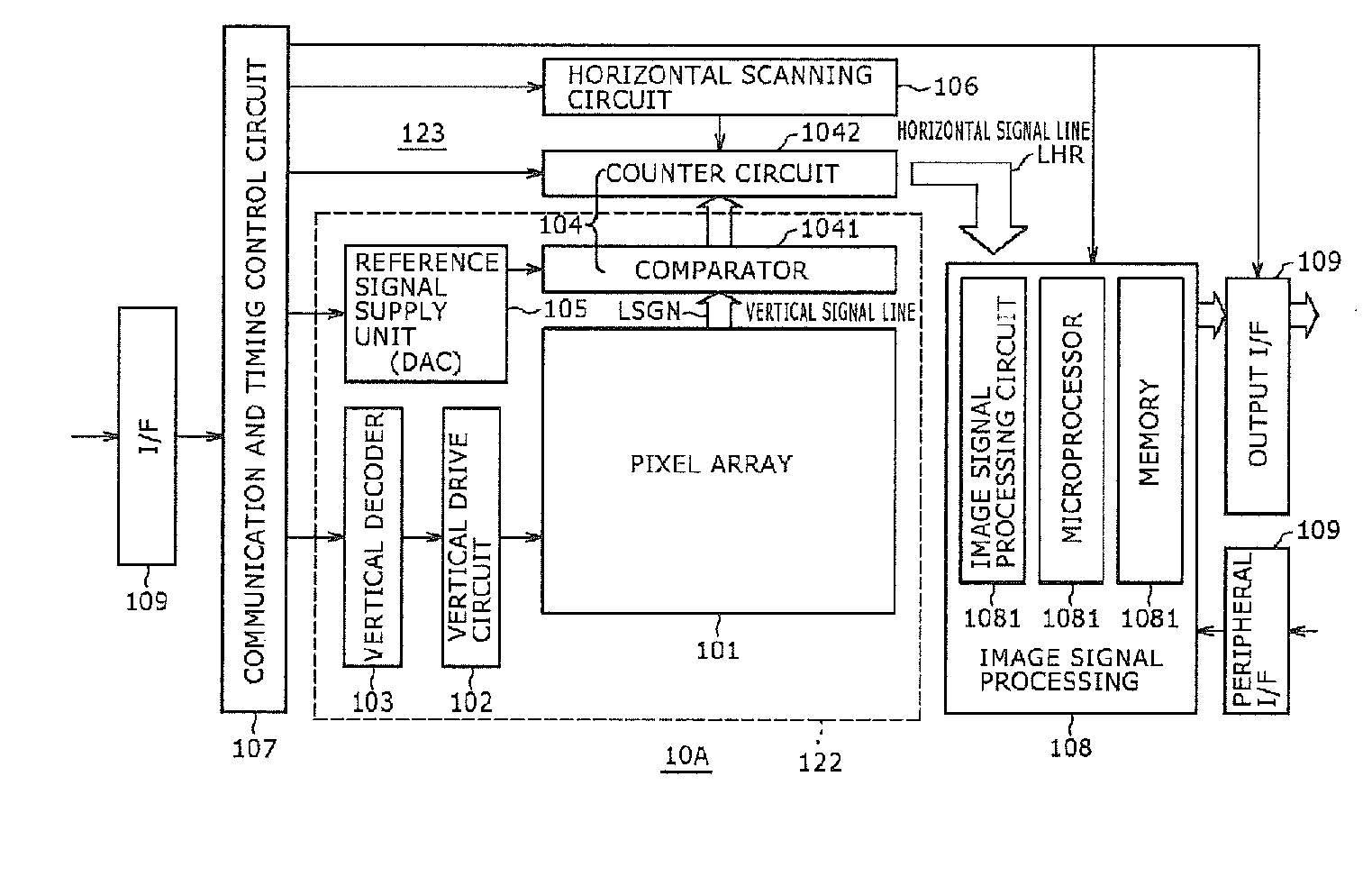
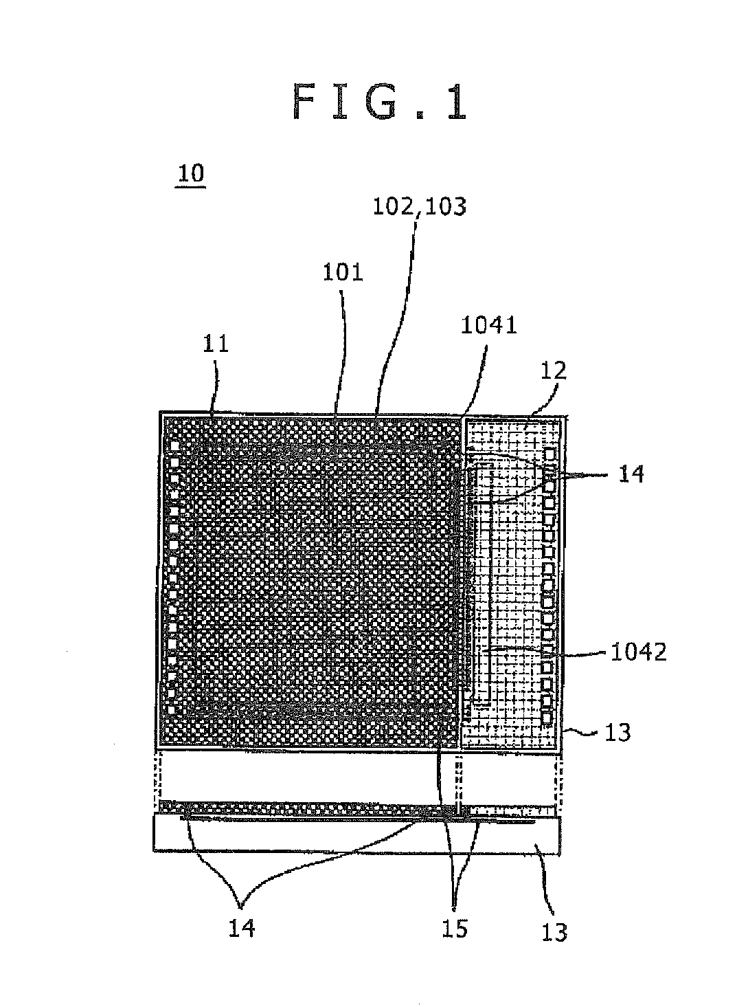
[0037]FIG. 1 is a diagram showing a configuration example of a solid-state imaging device as a semiconductor device relating to the embodiment of the present disclosure.

[0038]In the present embodiment, the configuration of a CMOS image sensor will be described as one example of the semiconductor device.

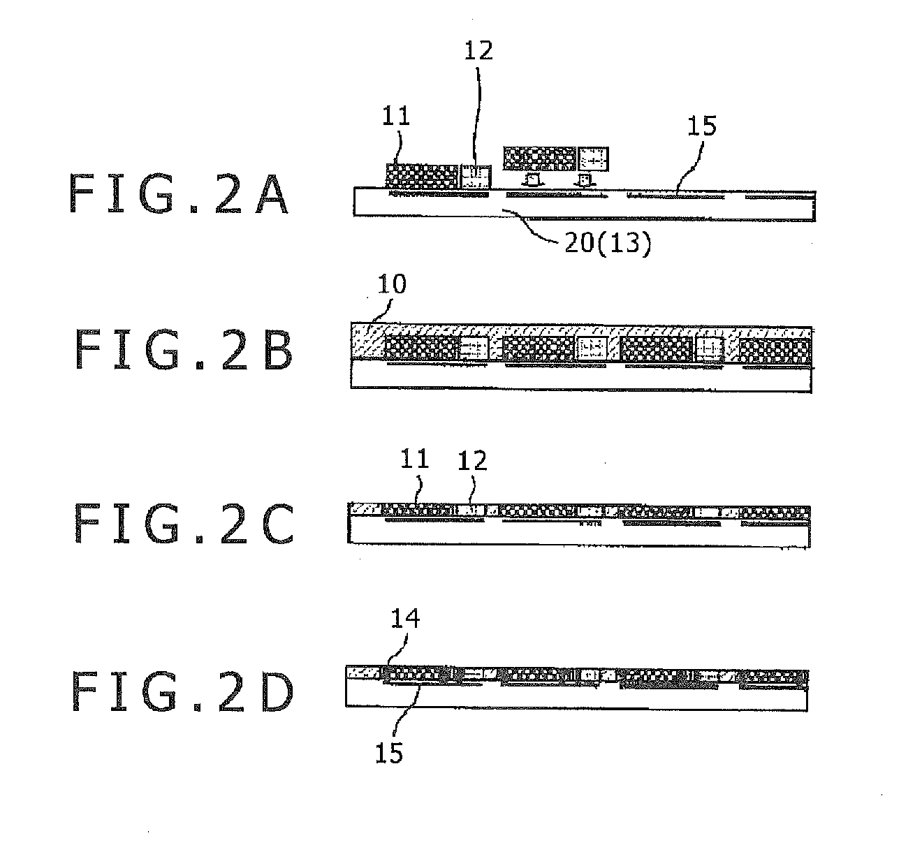
[0039]As shown in FIG. 1, in a solid-state imaging device 10, a first chip 11 and a second chip 12 are disposed in parallel on e.g. a support substrate (interposer) 13.

[0040]This solid-state imaging device 10 is characterized in that, as described later, an interconnect layer is provided on the support substrate 13 used ...


PUM


Abstract

Disclosed herein is a solid state imaging device including a support substrate; an imaging semiconductor chip having a pixel array disposed on the support substrate; and an image processing semiconductor chip disposed on the support substrate, wherein the imaging semiconductor chip and the image processing semiconductor chip are connected by through-vias, and interconnects formed on the support substrate.

Description

BACKGROUND ART[0001]The present disclosure relates to a semiconductor device having a stacking structure of two chips, a solid-state imaging device, and a camera system.[0002]Traditionally, for an imaging device, two chips, a CMOS image sensor (CIS) chip and an image processing chip, are each mounted in a package and assembly is carried out as a module.[0003]Alternatively, each chip is COB (Chip On Board) mounted in some cases.[0004]In recent years, in the case of mounting an imaging device in a cellular phone or the like, reduction in the mounting area and miniaturization are required, and an SOC (System-On-Chip) to integrate the above-described two chips into one chip has been developed.[0005]However, in the process in which the CIS process and the high-speed logic process are mixed for the integration into one chip, not only that the number of steps is increased and the cost is high but also that it is difficult to keep both of the analog characteristics and the logic characteris...

Claims


Application Information

Patent Timeline
Patent Type & Authority Applications(United States)
IPC IPC(8): H01L27/146H01L31/18
CPCH01L23/481H01L23/49827H01L27/14618H01L27/14683H01L27/14634H01L2924/13091H01L27/1469H01L2224/13H01L2924/00H01L25/04H01L27/146H01L23/48
Inventor SUKEGAWA, SHUNICHIFUKUSHIMA, NORIYUKI
Owner SONY CORP
Why Eureka
Try Eureka