Waveguide, method of manufacturing the same, and electromagnetic wave analysis apparatus

a technology of electromagnetic wave analysis and waveguides, which is applied in the direction of waveguides, waveguide horns, waveguides, etc., can solve the problems of increasing edge reflection or beam pattern divergence, physical and mechanical instability, and requiring an additional member, so as to improve the directivity of electromagnetic waves radiated from waveguides or guided to waveguides, and improve the frequency stability and handling of electromagnetic waves. , the effect of efficiently utilizing electromagnetic waves

Inactive Publication Date: 2013-03-14
CANON KK
View PDF3 Cites 29 Cited by
  • Summary
  • Abstract
  • Description
  • Claims
  • Application Information

AI Technical Summary

Benefits of technology

[0008]According to the present invention, the tapered structure having the spatial profile extending as described above is disposed at the part of the waveguide at which the electromagnetic wave exits or enters. More specifically, the tapered structure having the spatial profile extending in a lamination direction of a core layer as described above is disposed at an end of a plasmon waveguide. Thus, directivity of the electromagnetic wave radiated from the waveguide or guided to the waveguide is improved. In addition, because a directivity pattern of the electromagnetic wave can be set in the optical axis direction, it is expected to improve the frequency stability and handling of the electromagnetic wave. Therefore, it is expected by the present invention to realize a waveguide and the like capable of efficiently utilizing the electromagnetic wave.

Problems solved by technology

The DMW may cause an increase of edge reflection or beam pattern divergence due to mode mismatch between the waveguide and a space.
2840-2842 (2007) proposes a method of improving extraction efficiency and directivity by disposing a silicon lens at an end of the waveguide, but this method has practical problems such as being physically and mechanically unstable and requiring an additional member.
However, the structure can hardly be said to have sufficient physical and mechanical stability, and directivity of the electromagnetic wave may be tilted from an optical axis of the waveguide.

Method used


Image

  • Waveguide, method of manufacturing the same, and electromagnetic wave analysis apparatus
  • Waveguide, method of manufacturing the same, and electromagnetic wave analysis apparatus
  • Waveguide, method of manufacturing the same, and electromagnetic wave analysis apparatus

Examples


embodiment

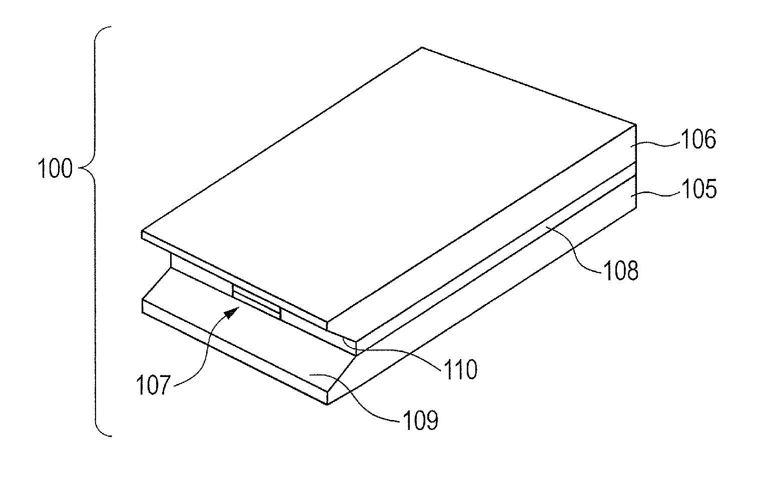
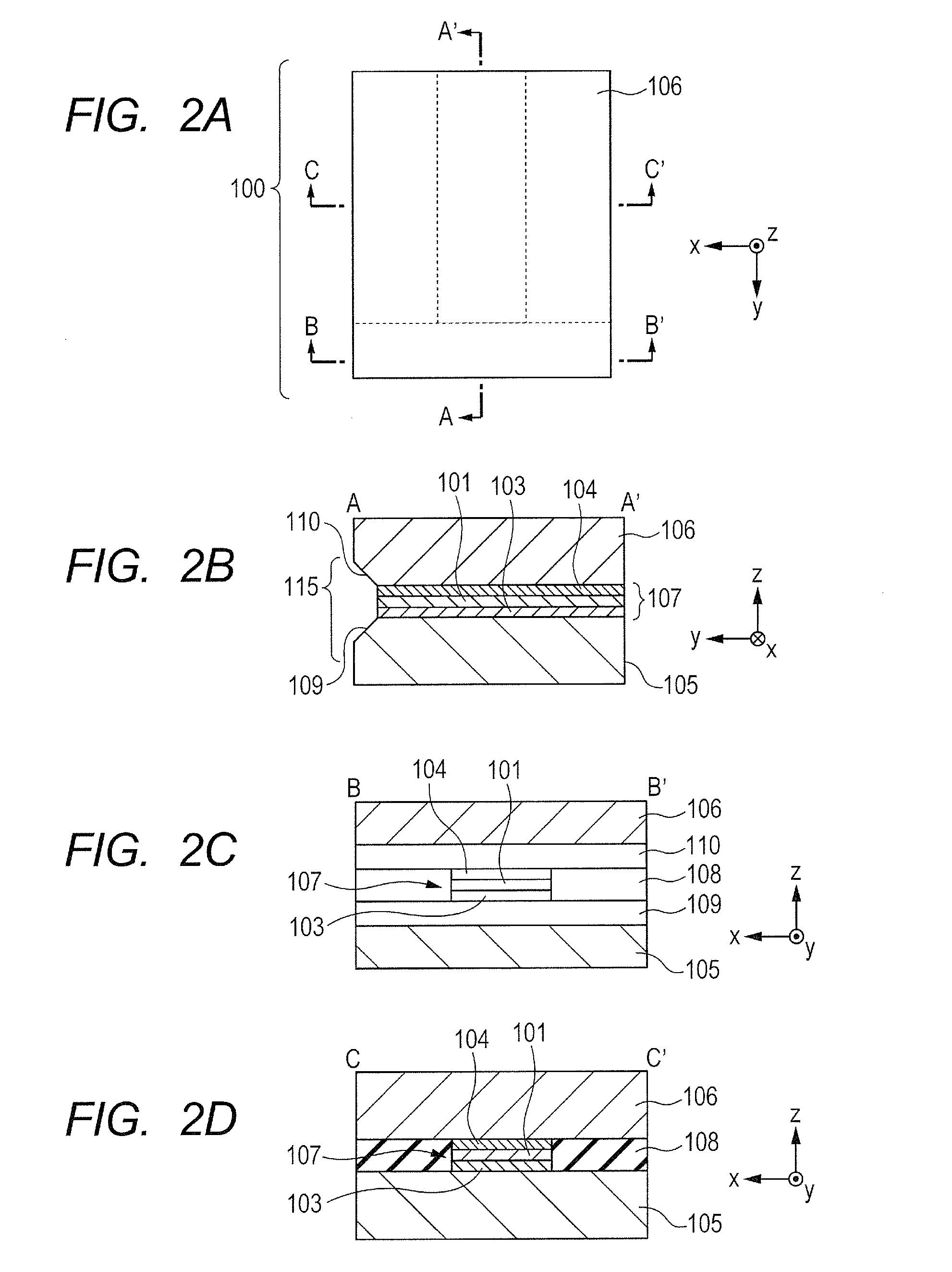
[0028]A waveguide 100 according to an embodiment of the present invention is described with reference to FIGS. 1 to 3C. FIG. 1 is a schematic diagram illustrating an external appearance of the waveguide 100. FIGS. 2A, 2B, 2C, and 2D are schematic diagrams illustrating a top view, an A-A′ cross-sectional view, a B-B′ cross-sectional view, and a C-C′ cross-sectional view of the waveguide 100, respectively. FIGS. 3A to 3C are schematic cross-sectional views of a modified example of this embodiment.

[0029]The waveguide 100 of this embodiment is an oscillation device including a waveguide structure 107 as a resonator, which is formed of and defined by an active layer 101 that is a core layer having an electromagnetic wave gain, a first conductor layer 103, and a second conductor layer 104. The waveguide structure 107 is integrated on a first substrate 105, a second substrate 106 is disposed on the waveguide structure107, and spacers 108 are disposed on the sides of the waveguide structure...

example 1

[0047]Specific Example 1 of the waveguide according to the present invention is described with reference to FIGS. 1 and 2A to 2D. Here, the waveguide according to the present invention can be used as a simple waveguide for electromagnetic waves, but it is possible to constitute the semiconductor device such as an oscillation device, an electromagnetic wave detection device, and an electromagnetic wave amplifying device by arranging the core layer to have an electromagnetic wave gain and nonlinearity. Therefore, in the following description, as an example thereof, there is described an example in which the waveguide of the present invention is used for the oscillation device. In this example, as the semiconductor multiple quantum well structure for generating terahertz waves by intersubband transition, an InGaAs / InAlAs-based resonant tunnel diode (RTD) structure which was lattice matched to an InP substrate was used. The RTD structure has a semiconductor multilayer structure in which...

example 2

[0058]A waveguide 500 according to Example 2 of the present invention is now described with reference to FIGS. 4 and 5A to 5D. An active layer 501 uses the quantum cascade laser structure disclosed in Appl. Phys. Lett. 83, 2124 (2003). The active layer 501 is a semiconductor multilayer at a thickness of about 10 μm. With regard to a first conductor layer 503 and a second conductor layer 504, the DMW structure is used. Further, with regard to other constituent materials such as a substrate 505, a substrate 506, and a spacer 508, the same configurations as in Example 1 are used, and those components are manufactured by substantially the same manufacturing method. In a waveguide structure 507, the conductor layers 503 and 504 are in a rectangular pattern of about 2.6 mm×0.15 mm, and are designed to obtain oscillation of about 3 THz. In this structure, the equivalent refractive index of the waveguide structure 507 when the oscillation frequency is 3 THz is about 3, and the guide wavelen...


PUM

PropertyMeasurementUnit
thicknessaaaaaaaaaa
acute angleaaaaaaaaaa
angleaaaaaaaaaa

Abstract

Provided is a waveguide for guiding an electromagnetic wave between a first conductor layer and a second conductor layer each having a negative dielectric constant real part for the electromagnetic wave, the waveguide including a tapered structure in a part of the waveguide at which the electromagnetic wave exits or enters, in which a spatial profile of the tapered structure perpendicular to an optical axis extends to both sides with respect to the optical axis at least in one direction orthogonal to the optical axis as being closer to an opening plane at an outermost part of the tapered structure.

Description

BACKGROUND OF THE INVENTION[0001]1. Field of the Invention[0002]The present invention relates to a waveguide, a method of manufacturing the same, and an electromagnetic wave analysis apparatus. In particular, the present invention relates to a waveguide for electromagnetic waves in frequency bands from a millimeter wave band to a terahertz wave band (30 GHz to 30 THz) (hereinafter referred to as terahertz waves), the waveguide configured to also be an oscillation device or a detection device, and methods for manufacturing the same.[0003]2. Description of the Related Art[0004]In the frequency band of terahertz waves, there are absorption peaks of many organic molecules in biological materials, medicines, electronic materials, and the like stemming from the structures and states thereof. Further, the terahertz waves easily penetrate materials such as paper, ceramic, resin, and cloth. In recent years, research and development have been conducted on imaging technology and sensing techno...

Claims


Application Information

Patent Timeline
Patent Type & Authority Applications(United States)
IPC IPC(8): G01N22/00H01P11/00H01P3/02G01N21/35G01N21/3563G01N21/3581H01Q13/02H01S1/02
CPCG01N21/3581G02B6/1226Y10T29/49016B82Y20/00G02B6/1228
Inventor KOYAMA, YASUSHI
Owner CANON KK
Why Eureka
Try Eureka