Semiconductor device and manufacturing method thereof

a semiconductor and semiconductor technology, applied in the direction of semiconductor devices, basic electric elements, electrical appliances, etc., can solve the problems of significant influence of contact resistance, achieve favorable ohmic contact, reduce resistance between a wiring layer and an oxide semiconductor layer, and improve the effect of ohmic conta

Active Publication Date: 2013-03-21
SEMICON ENERGY LAB CO LTD
View PDF2 Cites 37 Cited by
  • Summary
  • Abstract
  • Description
  • Claims
  • Application Information

AI Technical Summary

Benefits of technology

[0034]According to one embodiment of the present invention, a semiconductor device which maintains favorable electric characteristics and achieves miniaturization, and a manufacturing method thereof can be provided. Further, a semiconductor device in which resistance between a wiring layer and an oxide semiconductor layer is reduced so that a favorable ohmic contact can be obtained, and a manufacturing method thereof can be provided.
[0035]Further, according to one embodiment of the present invention, the size of a transistor can be sufficiently reduced. When the size of the transistor is...

Problems solved by technology

In the case of forming a miniaturized transistor, the contact area between the semiconductor layer and the conductive layer ...

Method used


Image

  • Semiconductor device and manufacturing method thereof
  • Semiconductor device and manufacturing method thereof
  • Semiconductor device and manufacturing method thereof

Examples


embodiment 1

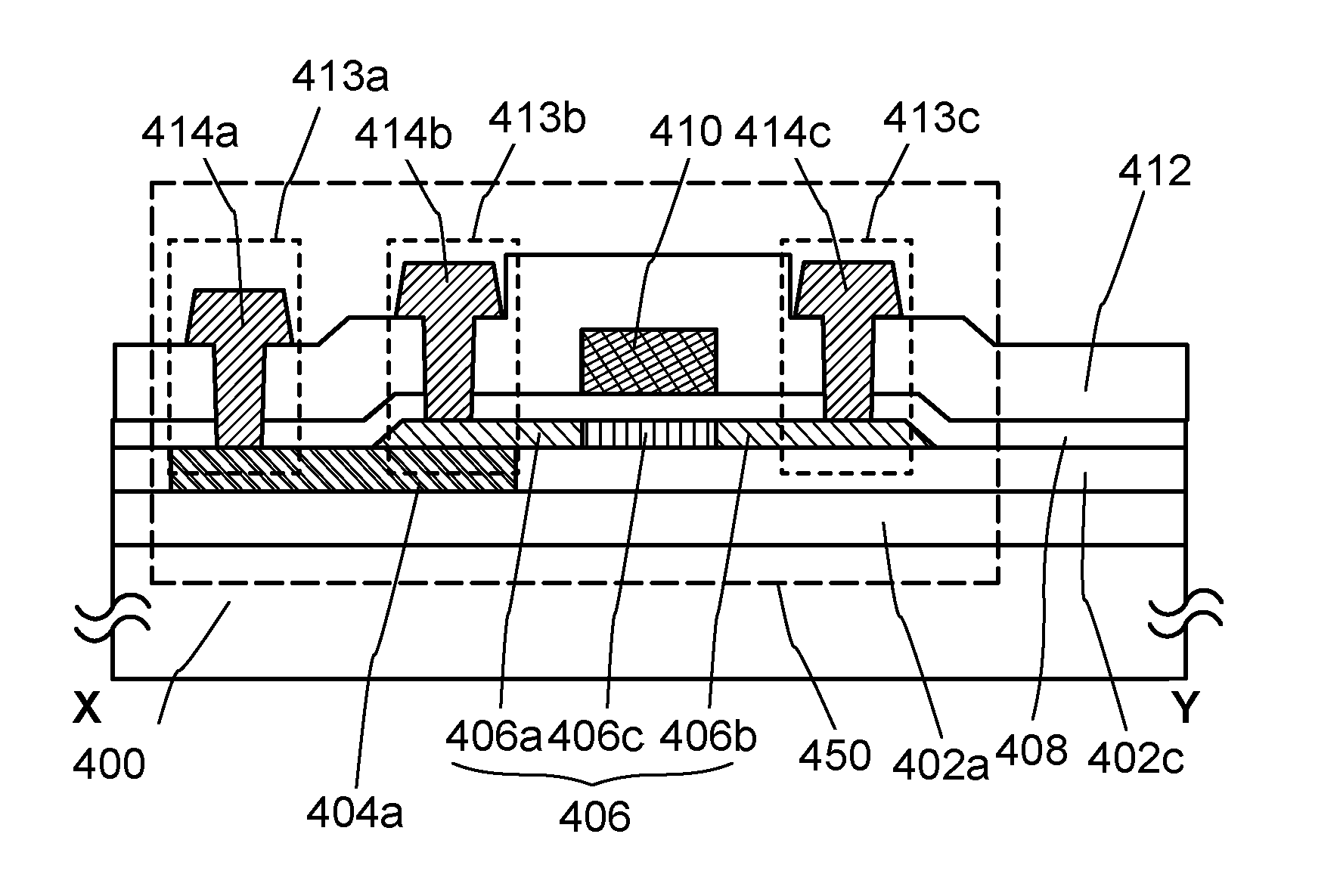
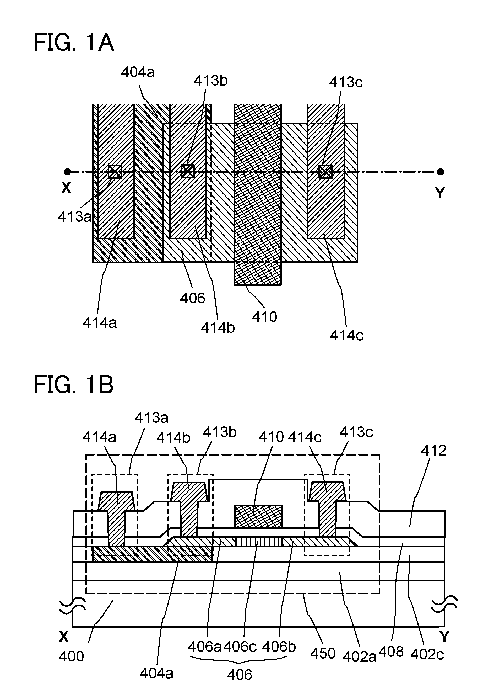
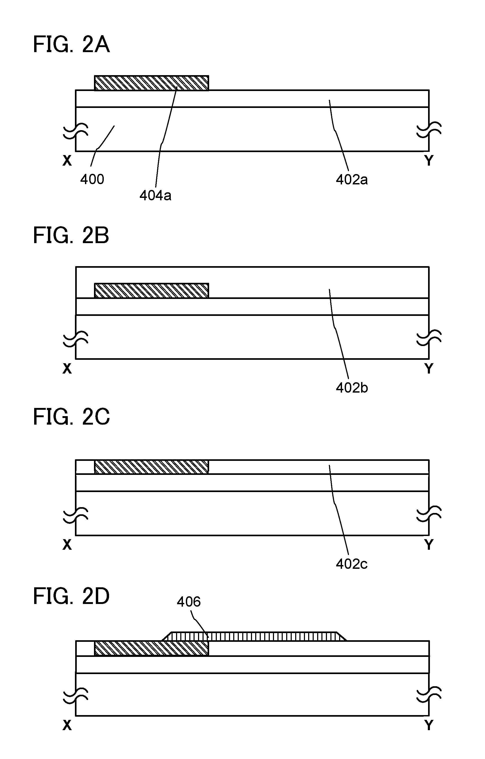
[0053]In this embodiment, a semiconductor device which is one embodiment of the present invention and a method for manufacturing the semiconductor device will be described with reference to FIGS. 1A and 1B, FIGS. 2A to 2D, and FIGS. 3A to 3C. In this embodiment, a top gate transistor will be described as an example of the semiconductor device.

[0054]FIGS. 1A and 1B are a plan view and a cross-sectional view of a transistor 450. FIG. 1A is a plan view and FIG. 1B is a cross-sectional view taken along line X-Y in FIG. 1A. Note that in FIG. 1A, some components of the transistor 450 (e.g., an insulating layer 412) are not illustrated for simplicity.

[0055]FIGS. 1A and 1B are an example of a structure of a semiconductor device manufactured by a method of this embodiment. The transistor 450 in FIGS. 1A and 1B includes a substrate 400, a base insulating layer 402a, a base insulating layer 402c, an electrode layer 404a, an oxide semiconductor layer 406 including a channel formation region 406...

embodiment 2

[0159]In this embodiment, a semiconductor device which is another embodiment of the present invention and a method for manufacturing the semiconductor device will be described with reference to FIGS. 4A and 4B, FIGS. 5A to 5D, and FIGS. 6A to 6C. In this embodiment, a top gate transistor will be described as an example of the semiconductor device.

[0160]FIGS. 4A and 4B are a plan view and a cross-sectional view of a transistor 460. FIG. 4A is a plan view and FIG. 4B is a cross-sectional view taken along line X-Y in FIG. 4A. Note that in FIG. 4A, some components of the transistor 460 (e.g., an insulating layer 412) are not illustrated for simplicity.

[0161]FIGS. 4A and 4B are an example of a structure of a semiconductor device manufactured by a method of this embodiment. The transistor 460 in FIGS. 4A and 4B includes a substrate 400, a base insulating layer 402a, a base insulating layer 402c, an electrode layer 404a, an electrode layer 404b, an oxide semiconductor layer 406 including a...

embodiment 3

[0201]In this embodiment, an example of a semiconductor device which includes the transistor described in Embodiment 1 or 2, which can hold stored data even when not powered, and which does not have a limitation on the number of write cycles, will be described with reference to drawings. Note that a transistor 162 included in the semiconductor device in this embodiment is the transistor described in Embodiment 1 or 2. Any of the structures of the transistors described in Embodiment 1 or 2 can be employed for the transistor 162.

[0202]Since the off-state current of the transistor 162 is small, stored data can be held for a long time owing to such a transistor. In other words, power consumption can be sufficiently reduced because a semiconductor storage device in which refresh operation is unnecessary or the frequency of refresh operation is extremely low can be provided.

[0203]FIGS. 8A to 8C illustrate an example of a structure of a semiconductor device. FIG. 8A is a cross-sectional vi...


PUM


Abstract

In a semiconductor device including an oxide semiconductor layer, a conductive layer is formed in contact with a lower portion of the oxide semiconductor layer and treatment for adding an impurity is performed, so that a channel formation region and a pair of low-resistance regions between which the channel formation region is sandwiched are formed in the oxide semiconductor layer in a self-aligned manner. Wiring layers electrically connected to the conductive layer and the low-resistance regions are provided in openings of an insulating layer.

Description

BACKGROUND OF THE INVENTION[0001]1. Field of the Invention[0002]The present invention relates to a semiconductor device and a manufacturing method thereof.[0003]In this specification, a semiconductor device generally means any device which can function by utilizing semiconductor characteristics, and an electro-optic device, a semiconductor circuit, and an electronic appliance are all included in the category of the semiconductor device.[0004]2. Description of the Related Art[0005]A technique by which transistors are formed using semiconductor thin films formed over a substrate having an insulating surface has attracted attention. The transistor is applied to a wide range of electronic devices such as an integrated circuit (IC) and an image display device (display device). A silicon-based semiconductor material is widely known as a material for a semiconductor thin film applicable to the transistor; in addition, an oxide semiconductor has attracted attention as another material.[0006...

Claims


Application Information

Patent Timeline
IPC IPC(8): H01L29/78H01L21/336
CPCH01L27/1225H01L29/7869H01L29/78618H01L29/41733
Inventor ISOBE, ATSUOSASAKI, TOSHINARI
Owner SEMICON ENERGY LAB CO LTD
Why Eureka
Try Eureka