Surface acoustic wave device
a surface acoustic wave and wave technology, applied in piezoelectric/electrostrictive/magnetostrictive devices, piezoelectric/electrostriction/magnetostriction machines, electrical equipment, etc., can solve problems such as unobtainable favorable frequency characteristics, achieve high-quality frequency characteristics of surface acoustic wave devices, prevent the scattering of surface acoustic waves and the like, and improve voltage resistance and frequency-temperature characteristics
- Summary
- Abstract
- Description
- Claims
- Application Information
AI Technical Summary
Benefits of technology
Problems solved by technology
Method used
Image
Examples
experimental examples
[0039]Surface acoustic wave devices having different IDT electrode dimensions as shown in Table 1 below were produced by causing exposure conditions at a resist mask formation for forming an IDT electrode to be variously different from each other. As a result of observing cross sections of the produced surface acoustic wave devices with a scanning electron microscope (SEM), a surface acoustic wave device in which no gap was observed between the IDT electrode and the dielectric film was evaluated as “G”, and a surface acoustic wave device in which a gap was observed between the IDT electrode and the dielectric film was evaluated as “NG”.
TABLE 1ExperimentalExampleRBTHTHBT / RHT / RResult10.50.480.430.120.030.860.24G20.50.290.430.120.150.860.24G30.50.340.440.080.100.880.16G40.50.380.460.100.100.920.2G50.50.490.460.120.010.920.24G60.50.490.470.080.010.940.16G70.50.500.470.080.010.940.16G80.50.470.470.080.030.940.16G90.50.380.470.080.030.940.16G100.50.410.470.080.050.940.16G110.50.500.470.08...
first modification
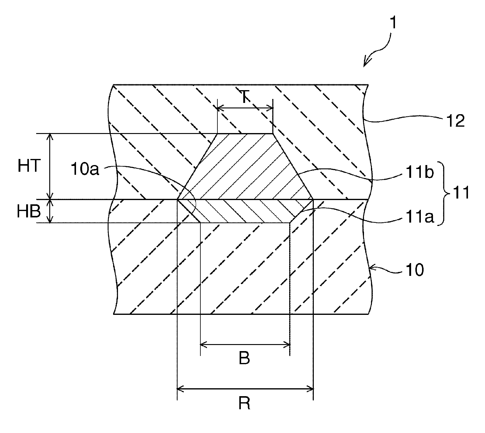
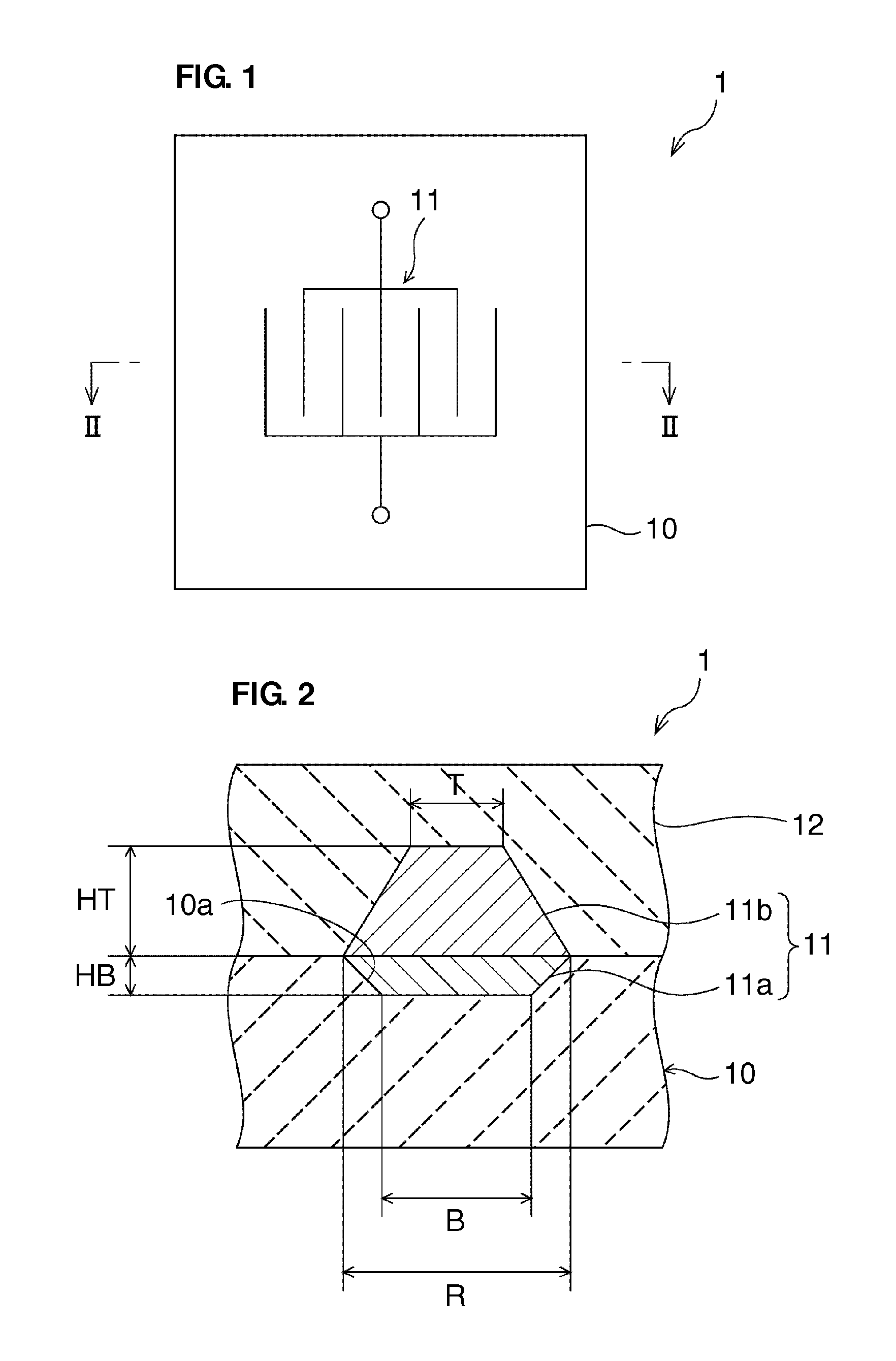
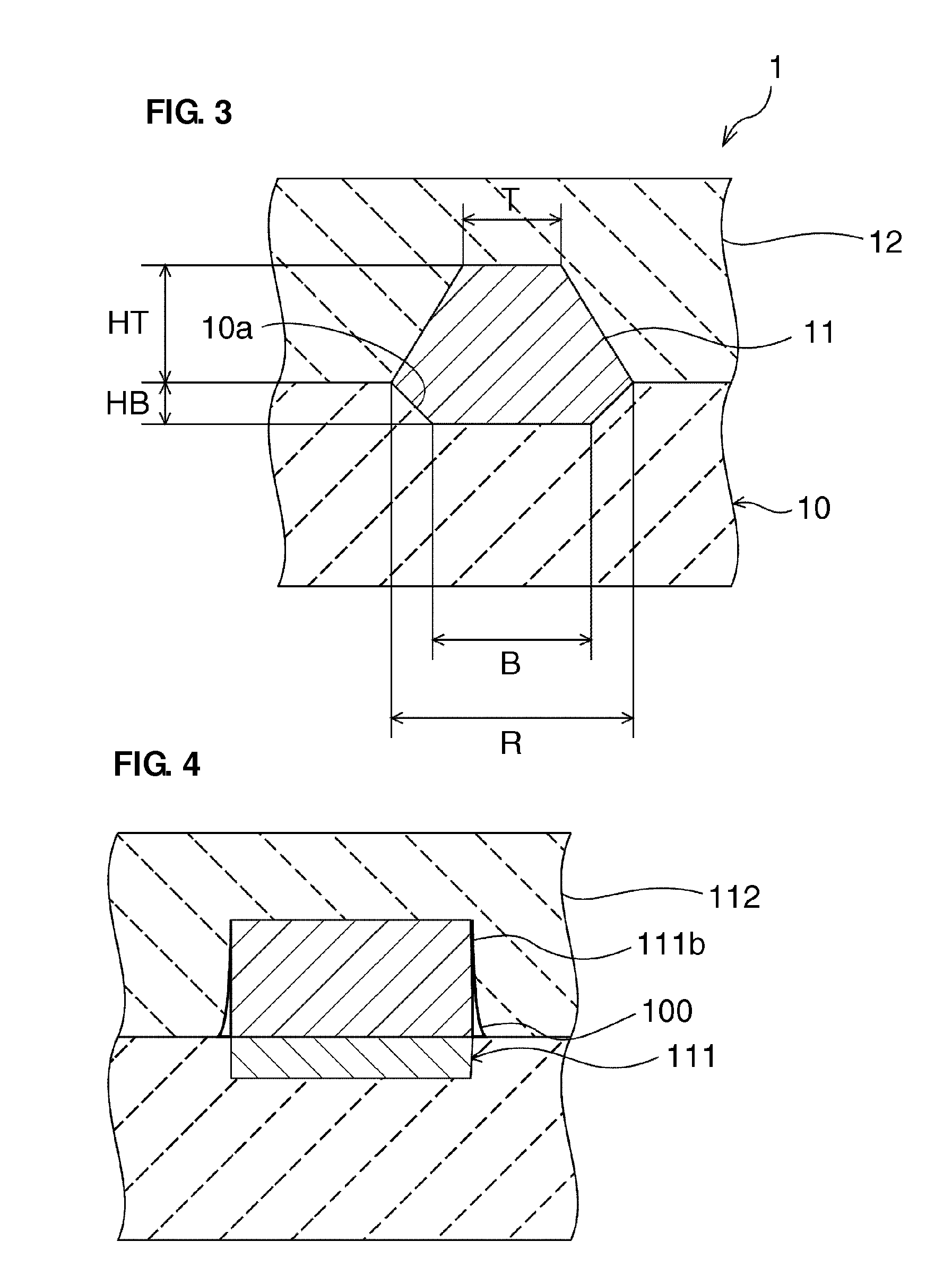
[0042]FIG. 3 is a schematic cross-sectional view of a surface acoustic wave device according to a first modification of a preferred embodiment of the present invention.
[0043]In the preferred embodiment described above, the case has been described where the IDT electrode 11 preferably includes the laminate of the first and second electrode layers 11a and 11b. However, the present invention is not limited to this configuration. For example, as shown in FIG. 3, the IDT electrode 11 may be composed of a single conductive layer.
PUM
 Abstract
Description
Claims
Application Information


