Semiconductor device

Inactive Publication Date: 2013-03-28
SEMICON ENERGY LAB CO LTD
View PDF8 Cites 34 Cited by
  • Summary
  • Abstract
  • Description
  • Claims
  • Application Information

AI Technical Summary

Benefits of technology

[0026]To realize a semiconductor device with higher performance, according to one embodiment of the present invention, a highly reliable structure for high-speed response and

Problems solved by technology

However, in such a structure of the transistor in which respective end portions of the source electrode and the drain electrode are aligned with or overlapped with an end portion of the gate electrode when seen in the top plane or the cross section, there is a problem of a short circuit between the gate electrode and the source electrode or th

Method used


Image

  • Semiconductor device
  • Semiconductor device
  • Semiconductor device

Examples


embodiment 1

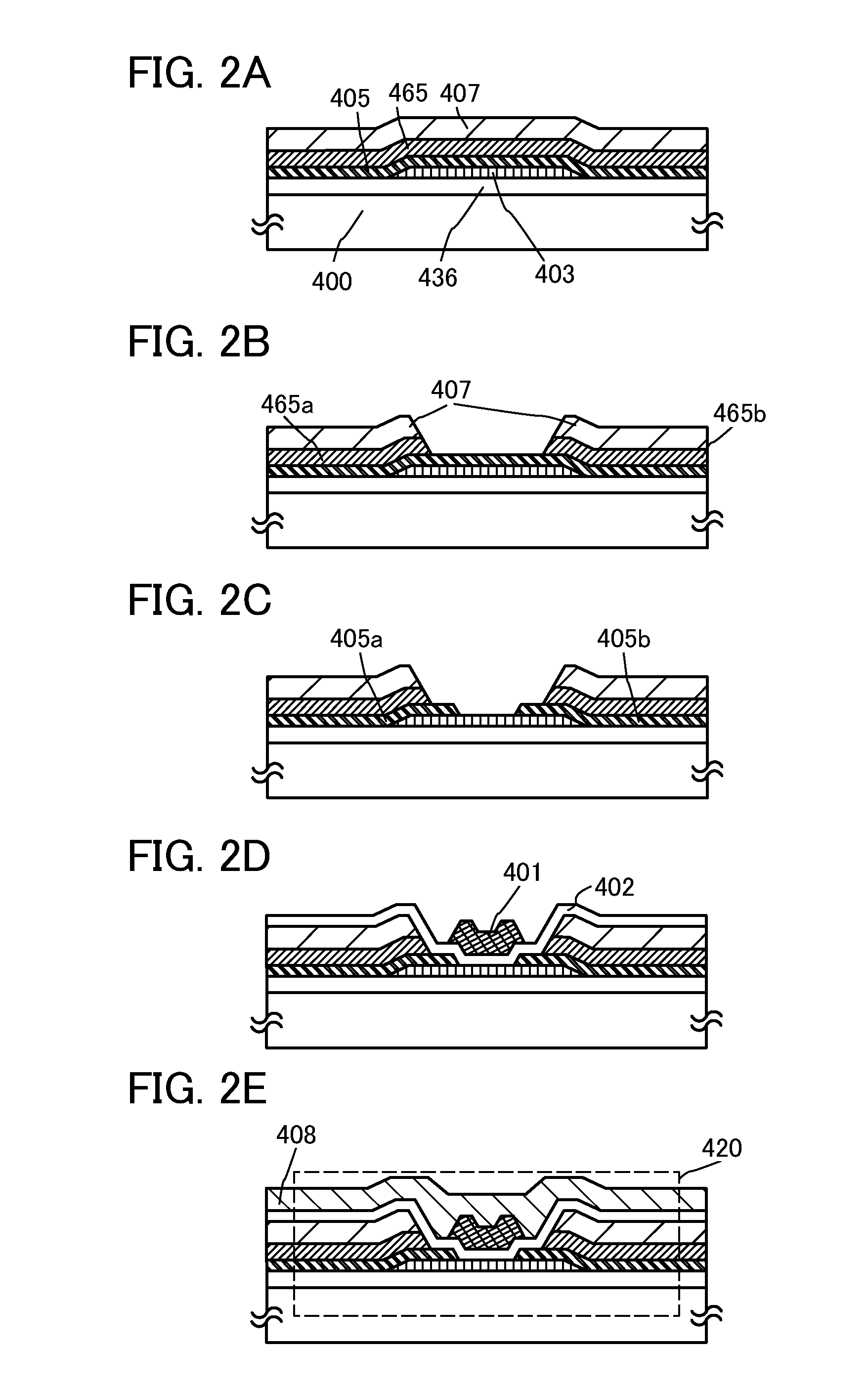
[0046]In this embodiment, a semiconductor device and a manufacturing method thereof according to one embodiment of the present invention are described using FIG. 1, FIGS. 2A to 2E, FIGS. 3A and 3B, and FIG. 4.

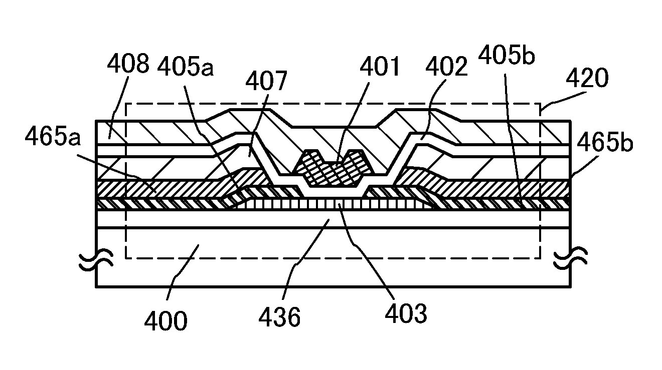
[0047]FIG. 1 is a cross-sectional diagram of a transistor 420 which is an example of a structure of a semiconductor device. The transistor 420 has a single-gate structure in which one channel formation region is formed, but instead may have a double-gate structure in which two channel formation regions are formed, or a triple-gate structure in which three channel formation regions are formed.

[0048]The transistor 420 includes, over a substrate 400 having an insulating surface, a buffer layer 436, an oxide semiconductor layer 403, first conductive layers 405a and 405b, second conductive layers 465a and 465b, an insulating layer 407, a gate insulating layer 402, a gate electrode layer 401, and an interlayer insulating layer 408 (see FIG. 1).

[0049]In the structure shown in FIG. 1 d...

embodiment 2

[0153]In this embodiment, another embodiment of the semiconductor device is described using FIGS. 5A and 5B and FIGS. 6A and 6B. The description of the above-described embodiment can apply to portions or steps which are the same as or have functions which are the same as those in the above-described embodiment, and repetitive description thereof is skipped. In addition, detailed description of the same portions is skipped.

[0154]FIG. 5A is a cross-sectional diagram of a transistor 440 which is an example which is different from the structure of the semiconductor device described in Embodiment 1.

[0155]The transistor 440 includes, over a substrate 400 having an insulating surface, an insulating layer 491 provided with embedded conductive layers 481a and 481b, an oxide semiconductor layer 403, first conductive layers 405a and 405b, second conductive layers 465a and 465b, a gate insulating layer 402, a gate electrode layer 401, and an interlayer insulating layer 408 (see FIG. 5A).

[0156]I...

embodiment 3

[0185]In this embodiment, another embodiment of the semiconductor device is described using FIGS. 7A to 7C. The description of the above-described embodiment can apply to portions or steps which are the same as or have functions which are the same as those in the above-described embodiment, and repetitive description thereof is skipped. In addition, detailed description of the same portions is skipped.

[0186]In this embodiment, FIG. 7A is a plane view of the transistor 420 shown in FIG. 1 described in Embodiment 1, FIG. 7B is a cross-sectional diagram along line X-Y in FIG. 7A, and FIG. 7C is a cross-sectional diagram along line V-W in FIG. 7A.

[0187]A structure of the transistor 420 shown in FIGS. 7A to 7C includes, like FIG. 1, over a substrate 400 having an insulating surface, a buffer layer 436, an oxide semiconductor layer 403, first conductive layers 405a and 405b, second conductive layers 465a and 465b, an insulating layer 407, a gate insulating layer 402, a gate electrode laye...


PUM


Abstract

A highly reliable structure for high-speed response and high-speed driving of a semiconductor device, in which on-state characteristics of a transistor are increased is provided. In the coplanar transistor, an oxide semiconductor layer, a source and drain electrode layers including a stack of a first conductive layer and a second conductive layer, a gate insulating layer, and a gate electrode layer are sequentially stacked in this order. The gate electrode layer is overlapped with the first conductive layer with the gate insulating layer provided therebetween, and is not overlapped with the second conductive layer with the gate insulating layer provided therebetween.

Description

TECHNICAL FIELD[0001]The present invention relates to a semiconductor device and a method for manufacturing the semiconductor device.[0002]In this specification, the semiconductor device means any device which can function by utilizing semiconductor characteristics, and an electrooptic device, a semiconductor circuit, and an electronic device are all included in the category of the semiconductor device.BACKGROUND ART[0003]Attention has been focused on a technique for forming a transistor using a semiconductor thin film formed over a substrate having an insulating surface (the transistor is also referred to as a thin film transistor (TFT)). The transistor has been widely applied to electronic devices such as an integrated circuit (IC) or an image display device (display device). A silicon-based semiconductor material is widely known as a material for a semiconductor thin film applicable to the transistor. As another material for the same, an oxide semiconductor has been attracting at...

Claims


Application Information

Patent Timeline
IPC IPC(8): H01L29/786
CPCH01L29/41733H01L29/7869H01L29/78618H01L29/42384H01L29/78645
Inventor YAMAZAKI, SHUNPEIISOBE, ATSUOOKAZAKI, YUTAKAHATANO, TAKEHISATEZUKA, SACHIAKIHONDO, SUGURUSAITO, TOSHIHIKO
Owner SEMICON ENERGY LAB CO LTD
Why Eureka
Try Eureka