Substrate processing apparatus, substrate processing method and storage medium

Active Publication Date: 2013-03-28
TOKYO ELECTRON LTD
View PDF21 Cites 17 Cited by
  • Summary
  • Abstract
  • Description
  • Claims
  • Application Information

AI Technical Summary

Benefits of technology

[0031]According to the second aspect of the present invention, the size of the substrate transfer mechanism can be reduced, whereby degree of freedom in layout of the positioning of the substrate tr

Problems solved by technology

However, the stage to which one transfer mechanism is accessible is limited

Method used


Image

  • Substrate processing apparatus, substrate processing method and storage medium
  • Substrate processing apparatus, substrate processing method and storage medium
  • Substrate processing apparatus, substrate processing method and storage medium

Examples


Example

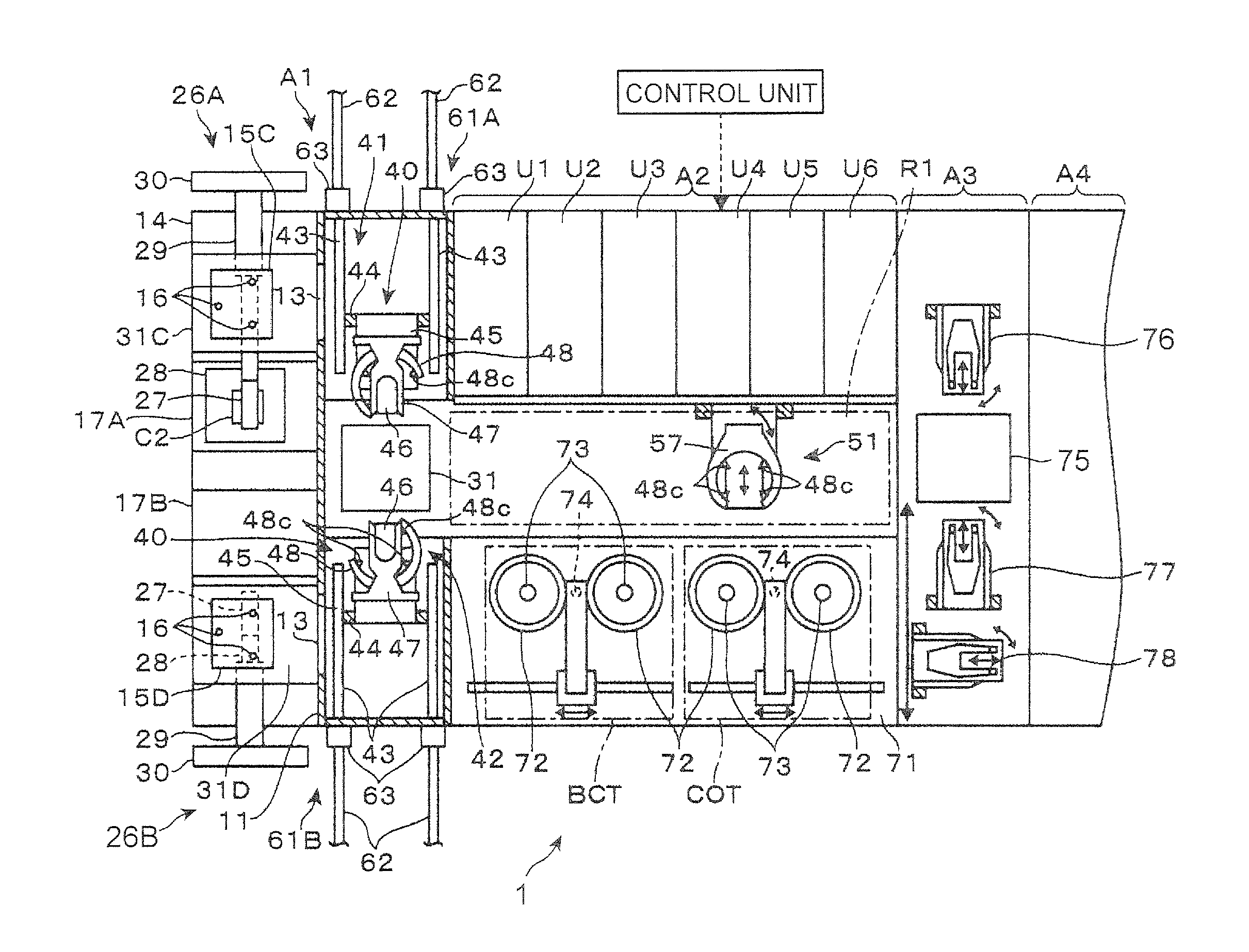
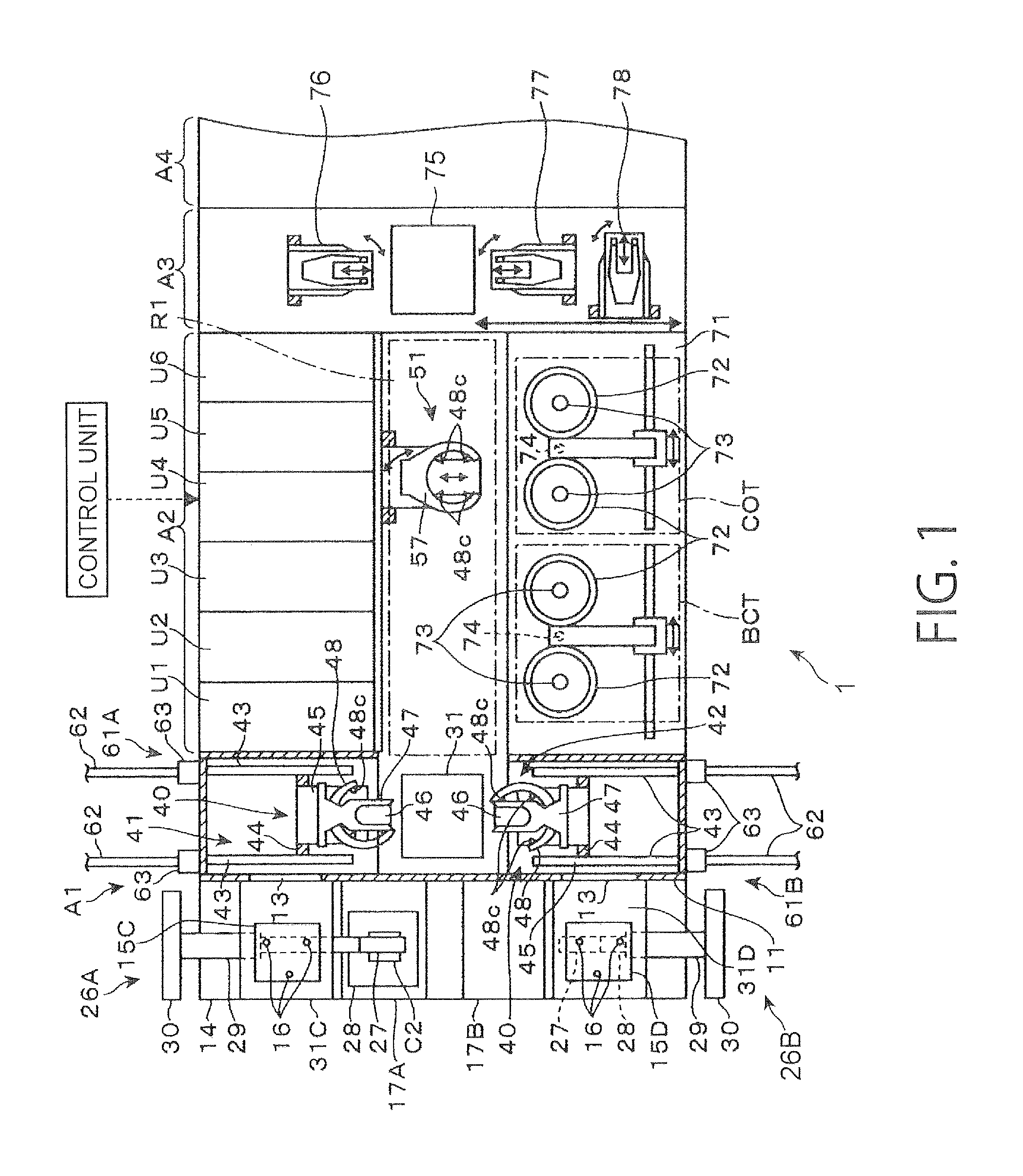
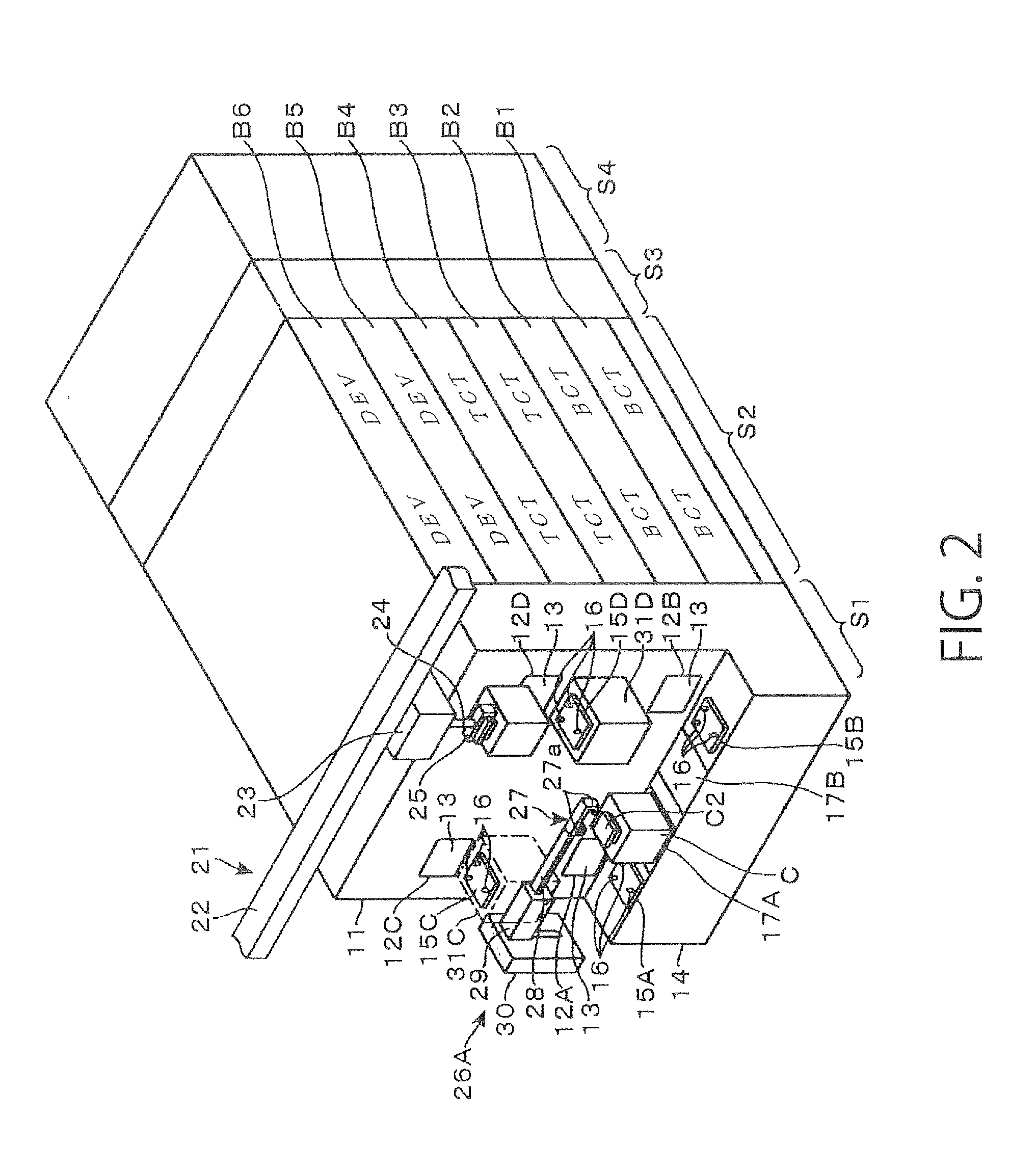
[0068]A first embodiment of the present invention will be firstly described. In the first embodiment, a substrate processing apparatus is constituted as a coating and developing apparatus 1. The coating and developing apparatus 1 is connected to an exposure apparatus, so as to form a resist-pattern formation system. FIG. 1 is a plan view of the resist-pattern formation system, FIG. 2 is a schematic perspective view thereof, and FIG. 3 is a schematic side view thereof. The coating and developing apparatus 1 is constituted by linearly connecting a carrier block A1, a processing block A2 and an interface block A3. An exposure apparatus A4 is further connected to the interface block A3 on a side opposed to the processing block A2. In this example, under conditions where a space between an exposure lens and a wafer W as a substrate is in a gas phase, the exposure apparatus A4 exposes the wafer W. The coating and developing apparatus 1 includes a processing module corresponding to such an...

Example

Second Embodiment

[0126]Herebelow, other embodiments are described, focusing on differences from the first embodiment. FIG. 18 is a front view of the carrier block A5 in the second embodiment. The carrier block A5 includes carrier moving mechanisms 81A and 81B, instead of the carrier moving mechanisms 26A and 26B. The support platform 14 has groove portions 82 and 82 extending from positions corresponding to the aforementioned temporary placement units 17A and 17B toward the carrier placement units 15A and 15B. There are provided carrier bottom-surface support units 83 constituting the carrier moving mechanisms 81A and 81B in the groove portions 82 and 82, respectively.

[0127]Since the carrier moving mechanism 81A and 81B have the same structure, the carrier moving mechanism 81A is described as a representative, with reference also to FIG. 19 showing a plan view thereof. The carrier bottom-surface support unit 83 is configured to be movable in the right and left direction along the g...

Example

Third Embodiment

[0131]FIGS. 22 and 23 are a front view and a longitudinal sectional plan view of a carrier block A6 in a third embodiment. The carrier block A6 differs from the carrier block A1 in that the carrier block A6 does not have the upper support platforms 31C and 31D, and that the support platform 14 is formed to extend from a front surface side to side surface sides of the carrier block A6. The transport openings 12C and 12D for wafer W are formed in the side surfaces of the carrier block A6. The transport openings 12A to 12D are disposed at the same height, for example. The carrier placement units 15C and 15D are provided correspondingly to the transport openings 12C and 12D. When the carrier block A6 is viewed from the front side, the carrier placement units 15C and 15D are configured to be movable between the unloading position and the loading position in the right and left direction. In this example, corner parts of the support platform 14 are formed as the temporary ...


PUM


Abstract

A substrate processing apparatus includes: a carrier block including first and second carrier placement units spaced apart in a right and left direction; a processing block having a layered structure in which a plurality of layered parts are vertically arranged, the layered parts each including a substrate transport mechanism for transporting a substrate and a processing module for processing a substrate; a tower unit including plural substrate placement units located at height positions where a substrate is transferred by the substrate transport mechanism of the layered part corresponding to the substrate placement unit; a first substrate transfer mechanism configured to transfer a substrate between the carrier on the first carrier placement unit and the substrate placement unit of the tower unit; and a second substrate transfer mechanism configured to transfer a substrate between the carrier on the second substrate placement unit and the substrate placement unit of the tower unit.

Description

CROSS REFERENCE TO RELATED APPLICATIONS[0001]This application is based upon and claims the benefits of priorities from the prior Japanese Patent Application No. 2011-208097 filed on Sep. 22, 2011 and Japanese Patent Application No. 2011-208100 filed on Sep. 22, 2011, the entire contents of which are incorporated herein by reference.BACKGROUND OF THE INVENTION[0002]1. Field of the Invention[0003]The present invention relates to a substrate processing apparatus, a substrate processing method and a storage medium, in which a substrate is taken out from a carrier and processed.[0004]2. Background Art[0005]A photoresist process, which is one of semiconductor manufacturing processes, is performed by a substrate processing apparatus including a carrier block for holding a carrier accommodating a plurality of semiconductor wafers (hereinafter referred to as “wafers”) and a processing block for processing a wafer sent from the carrier block.[0006]The processing block is sometimes formed by v...

Claims


Application Information

Patent Timeline
IPC IPC(8): B05C13/00B25J9/00B05C11/00
CPCH01L21/67178H01L21/67745H01L21/67766Y10S414/139H01L21/67781H01L21/68707Y10S414/137H01L21/67769
Inventor ENOKIDA, SUGURUNAKAHARADA, MASAHIROMIYATA, AKIRAKIYAMA, HIDEKAZUIIDA, NARUAKI
Owner TOKYO ELECTRON LTD
Why Eureka
Try Eureka