Semiconductor device and display device equipped with same

a technology of semiconductor devices and display devices, which is applied in the direction of semiconductor devices, electrical appliances, transistors, etc., can solve the problems of difficult to make crystalline silicon film thick, low sensitivity, and low productivity, so as to increase the effective sensitivity of the photosensor, increase the intensity of the incident light, and increase the amount of light absorbed

Inactive Publication Date: 2013-04-04
SHARP KK
View PDF5 Cites 13 Cited by
  • Summary
  • Abstract
  • Description
  • Claims
  • Application Information

AI Technical Summary

Benefits of technology

[0030]According to the present invention, in a semiconductor device provided with a photosensor part that includes a thin film diode and a thin film transistor on the same substrate, light reflected by the inclined surface of the metal layer can be made incident upon the semiconductor layer of the thin film diode. As a result, it is possible to increase the intensity of the light incident upon the thin film diode. Also, the light reflected off of the inclined surface of the metal layer enters the semiconductor layer from a side face of the semiconductor layer of the thin film diode and is transmitted towards the in-plane direction of the semiconductor layer, and thus, the light path in the semiconductor layer is longer than when the light is radiated from the perpendicular direction. Therefore, it is possible to increase the amount of light absorbed by the semiconductor layer of the thin film diode, thus increasing the effective sensitivity of the photosensor.
[0031]In particular, it is possible to reliably increase the effective sensitivity of the photosensor part to infrared light when conducting sensing using infrared light.
[0032]Also, according to the present invention, it is possible to manufacture the above-mentioned semiconductor device with ease without increasing the number of manufacturing steps or manufacturing cost, and so as to be more compact, higher performance, and lower cost.

Problems solved by technology

In such a case, because the TFD semiconductor layer (low temperature polysilicon layer) is thin, the TFD semiconductor layer cannot absorb a sufficient amount of relatively long wavelength light (infrared light, for example), which means that there is a possibility that a high sensitivity cannot be attained.
However, when making the semiconductor layer made of low temperature polysilicon thicker, there is a possibility that productivity is reduced because the crystallization process such as laser crystallization conducted on an amorphous silicon film requires longer time.
In particular, when conducting crystallization of the amorphous silicon film using a catalyst element, it is difficult to make the crystalline silicon film thick as stated above.
Thus, in the past, it was difficult to achieve desired TFT characteristics while ensuring the desired sensitivity of photosensors that use TFDs when a TFT and a TFD were formed using the same semiconductor film.

Method used


Image

  • Semiconductor device and display device equipped with same
  • Semiconductor device and display device equipped with same
  • Semiconductor device and display device equipped with same

Examples


embodiment 1

[0050]Embodiment 1 of a semiconductor device of the present invention will be described below. The semiconductor device of the present embodiment is a liquid crystal display device having a photosensor part using a thin film diode and a thin film transistor, for example.

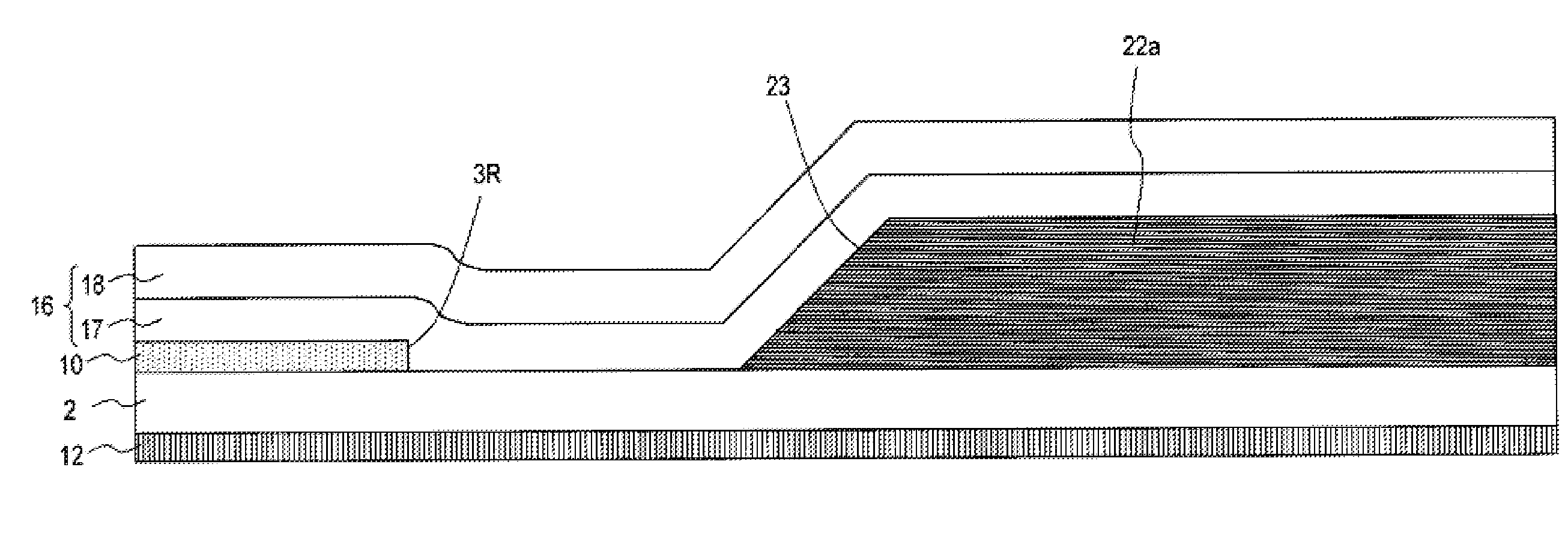
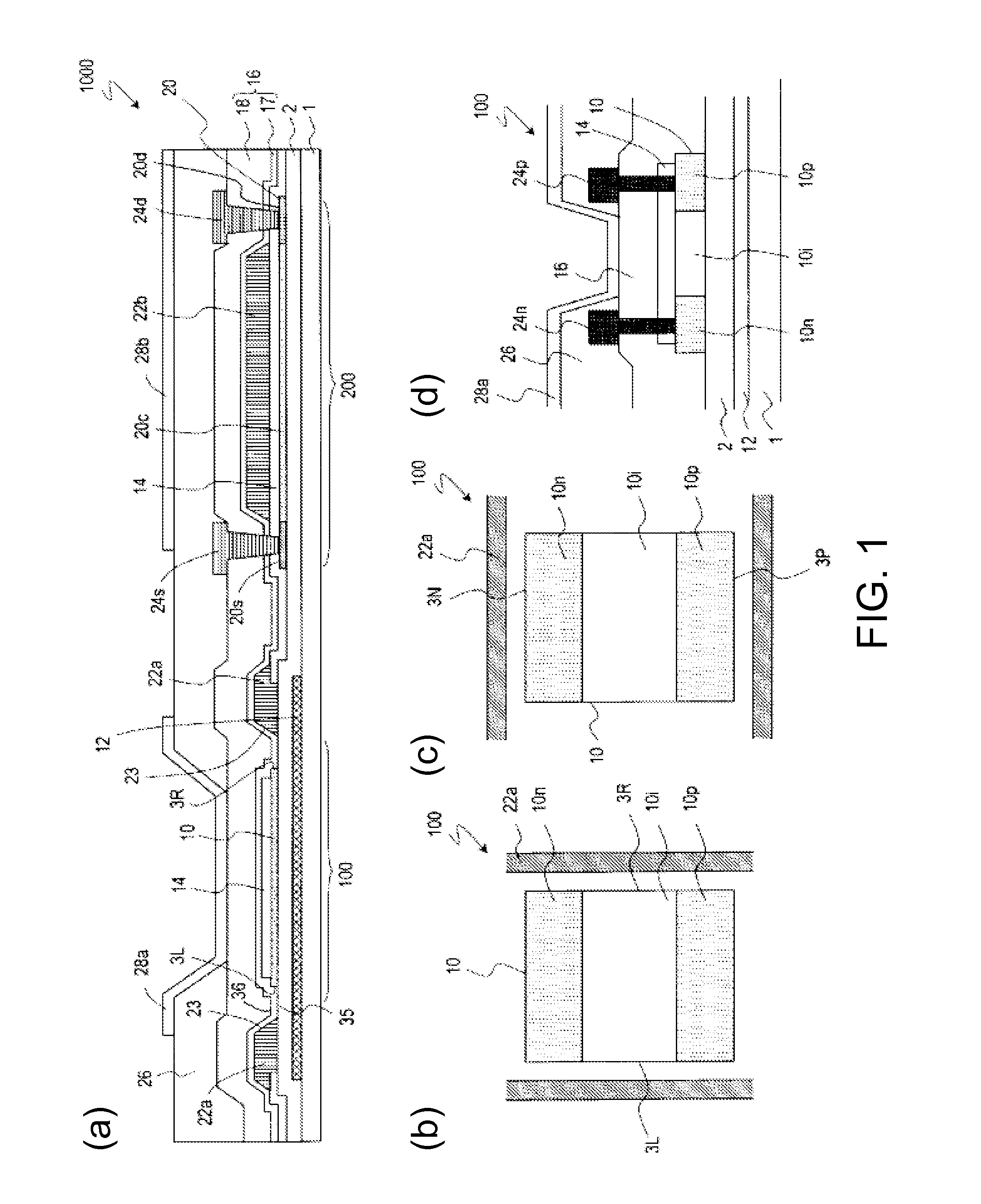
[0051]FIG. 1(a) is a schematic cross-sectional view that shows a thin film diode 100 and a thin film transistor 200 in a semiconductor device 1000 of the present embodiment. FIGS. 1(b) and 1(c) are schematic plan views that show examples of configurations of the thin film diode 100. FIG. 1(d) is a schematic cross-sectional view of the thin film diode 100.

[0052]As shown in FIG. 1(a), the semiconductor device 1000 is provided with a substrate 1, a photosensor part including the thin film diode 100 formed on the substrate 1, and the thin film transistor 200. The photosensor part may be disposed in the display region of the liquid crystal display device. The thin film transistor 200 may be a pixel switching TFT disposed ...

embodiment 2

[0144]The present embodiment describes a display device provided with a sensor function.

[0145]The display device provided with a sensor function of the present embodiment is a liquid crystal display device with a touch sensor, for example, and has a display region and a frame region located in the periphery of the display region. The display region has a plurality of display parts (pixels) and a plurality of photosensor parts. Each display part includes a pixel electrode and a pixel switching TFT, and each photosensor part includes a photosensor TFD that detects light that includes infrared light (wavelength: 850 nm), for example. The frame region is provided with a display driver circuit for driving each display part, and a driver circuit TFT is used for the driver circuit. The pixel switching TFT, the driver circuit TFT, and the photosensor part TFD are formed on the same substrate. In the display device of the present invention, at least one of the TFTs used in the display device...


PUM


Abstract

Disclosed is a semiconductor device 1000 including a substrate 1, a thin film diode 100 that is supported by the substrate 1 and has a first semiconductor layer 10 having a light-receiving region 10i, a thin film transistor 200 that is supported by the substrate 1 and has a second semiconductor layer 20, and a metal layer 22a that has an inclined surface 23 that is inclined to the surface of the substrate 1, in which the thin film diode 100 can detect light that enters the light-receiving region 10i and has a prescribed wavelength, in which both the first semiconductor layer 10 and the second semiconductor layer 20 are composed of the same semiconductor film, and in which the inclined surface 23 of the metal layer 22a faces at least a part of the side faces 3R and 3L of the first semiconductor layer 10. This constitution enables an increase in the amount of light absorbed by the thin film diode and an improvement in the effective light reception sensitivity of an optical sensor part.

Description

TECHNICAL FIELD[0001]The present invention relates to a semiconductor device that includes a thin film diode (TFD) and a display device equipped with the same.BACKGROUND ART[0002]In recent years, development of electronic devices such as display devices, image sensors, and the like provided with a photosensor part that uses a TFD has been in progress.[0003]Patent Document 1 discloses an image sensor in which a photosensor part that uses a TFD and a driver circuit that uses a thin film transistor (TFT) are provided on the same substrate. Patent Document 2 discloses a display device provided with an optical touch panel. This display device can detect that an object such as a finger is in contact with a display surface using external light by providing photosensor parts that use TFDs in a display region of a liquid crystal display device. Patent Document 3 discloses a display device provided with an optical touch panel that detects that an object such as a finger is in contact with a d...

Claims


Application Information

Patent Timeline
Patent Type & Authority Applications(United States)
IPC IPC(8): H01L29/786
CPCH01L27/1214H01L29/786H01L27/1446
Inventor AICHI, HIROSHI
Owner SHARP KK
Why Eureka
Try Eureka