

CMOS image sensor with reset shield line
a technology of image sensor and shield line, which is applied in the field of image sensors, can solve the problems of serious limitation on improving image sensor performan
- Summary
- Abstract
- Description
- Claims
- Application Information
AI Technical Summary
Benefits of technology
Problems solved by technology
Method used
Image

Examples
Embodiment Construction
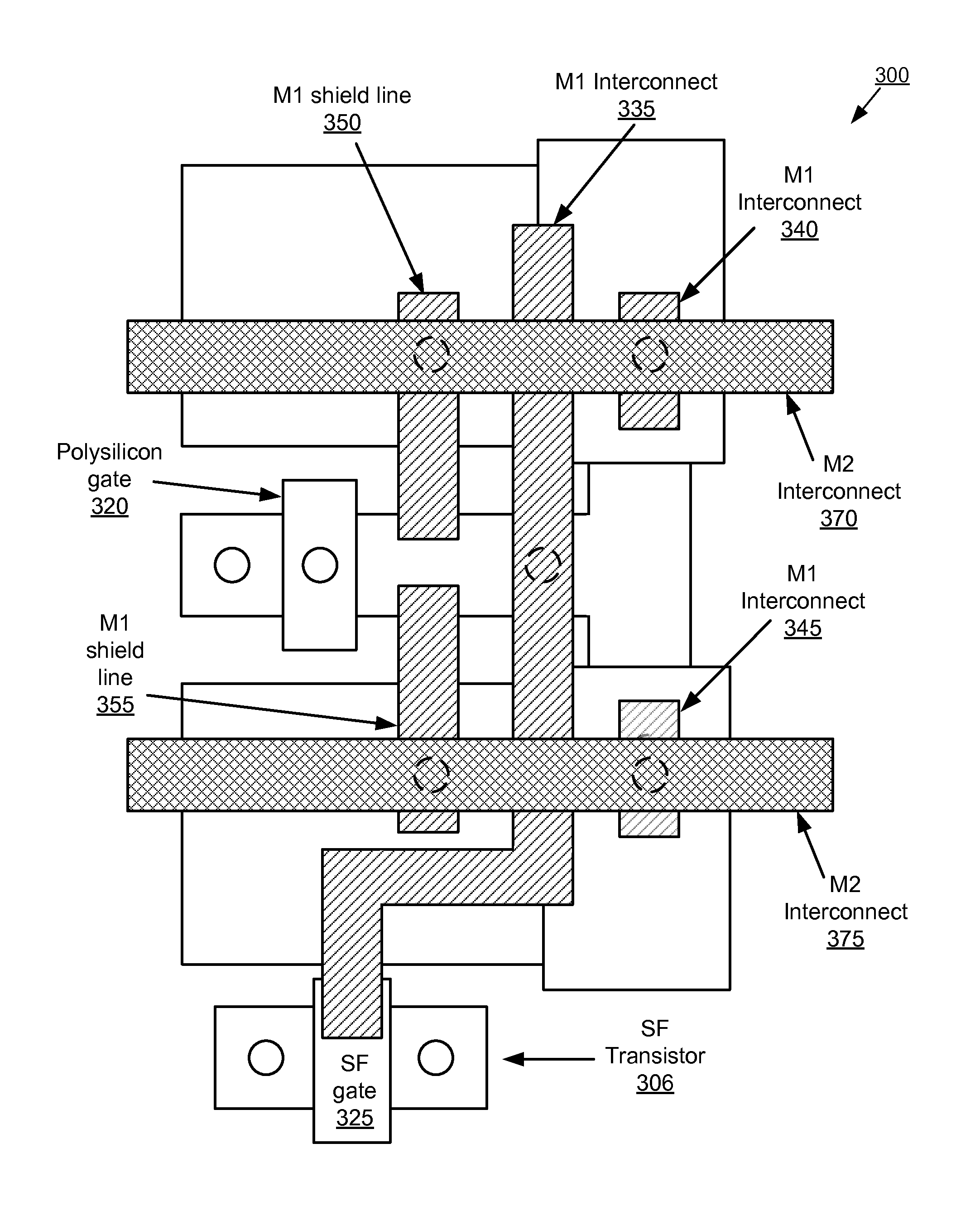
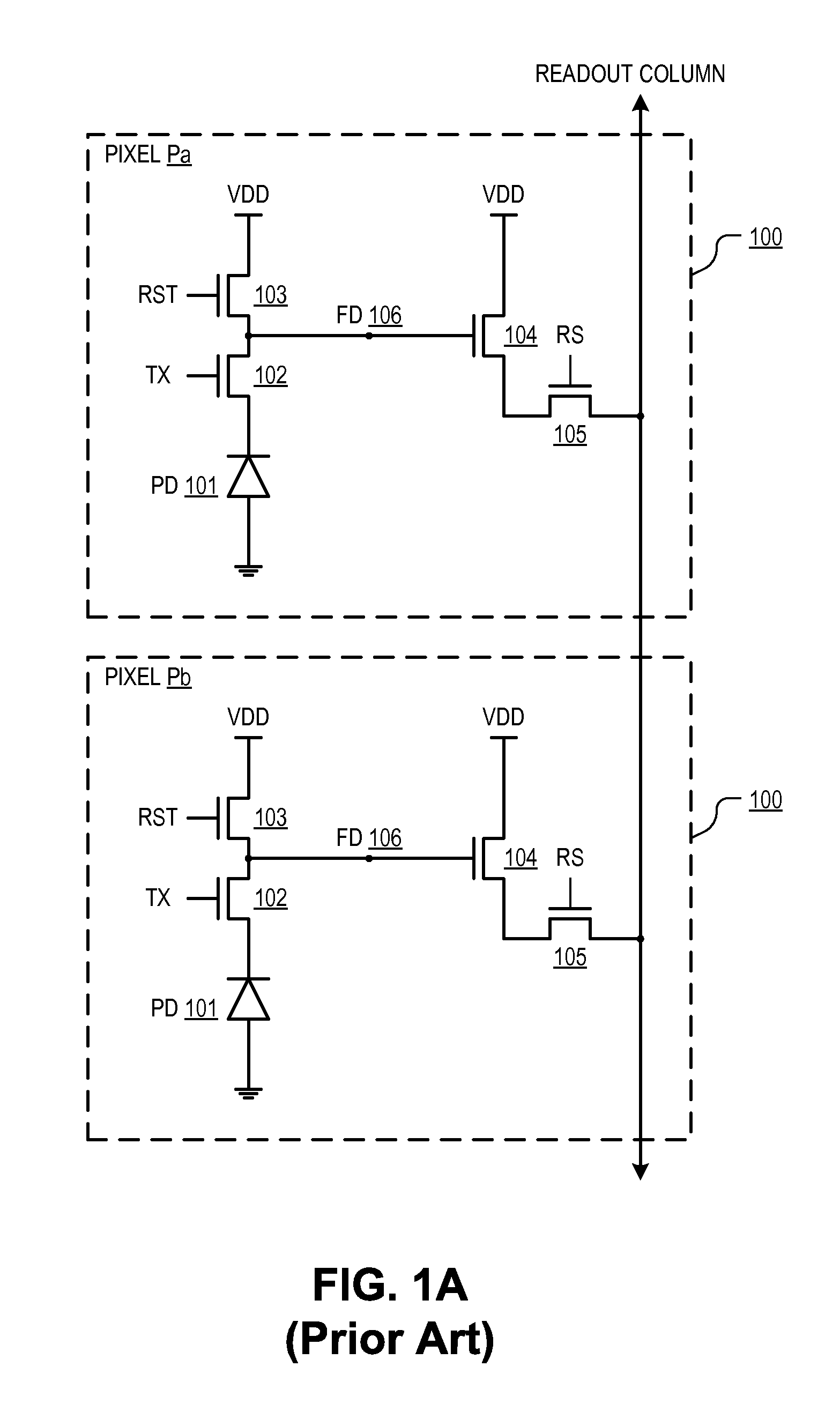
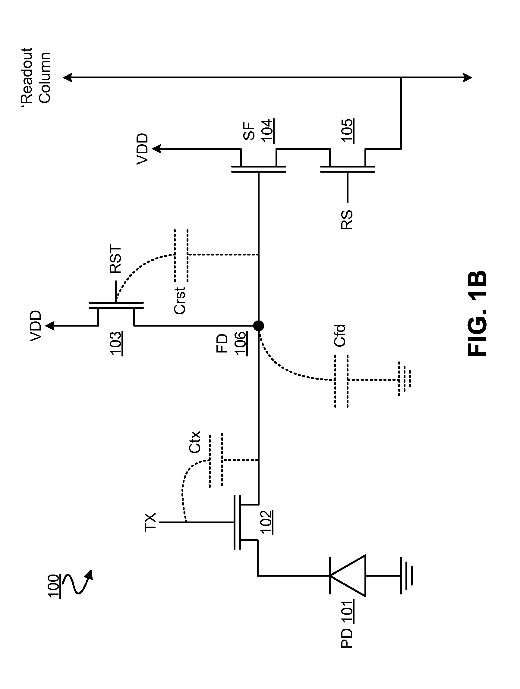
[0019]FIG. 1B illustrates properties of pixel cell 100—e.g. in FIG. 1A—which affect image sensing performance in a conventional image sensor. More particularly, operation of pixel cell 100 may be affected by one or more of (1) a transfer capacitance (Ctx) between the gate of transfer transistor 102 and floating diffusion node 106, (2) a reset capacitance (Crst) between the gate of reset transistor 103 and floating diffusion node 106, and (3) a floating node capacitance (Cfd) between floating diffusion node 106 and ground.
[0020]After a pixel reset, the potential well at floating diffusion node 106 needs to be sufficiently low—e.g. as compared to the potential at photodiode 101—to avoid signal charge from photodiode 101 overflowing at floating diffusion node 106, causing some of the signal charge to flow back into photodiode 101. This unintended charge sharing tends to result in image lag.
[0021]Successive generations of smaller and smaller pixel structures tend to exhibit less and les...
PUM
 Abstract
Description
Claims
Application Information