Semiconductor device

Active Publication Date: 2013-04-04
ABLIC INC
View PDF16 Cites 3 Cited by
  • Summary
  • Abstract
  • Description
  • Claims
  • Application Information

AI Technical Summary

Benefits of technology

[0013]In an IC having multi-layered wirings formed therein, a moisture entering path from the SOG layer between the laminated interlayer insulating films, which is a cause for degr

Problems solved by technology

In the etch back technology, however, the SOG layer 314 is present between the laminated interlayer insulating films, and hence moisture may enter through the SOG layer to cause fluctuations in element characteristics of an IC, resulting in a problem i

Method used


Image

  • Semiconductor device
  • Semiconductor device
  • Semiconductor device

Examples


Embodiment Construction

[0025]Referring to the accompanying drawings, an embodiment of the present invention is hereinafter described.

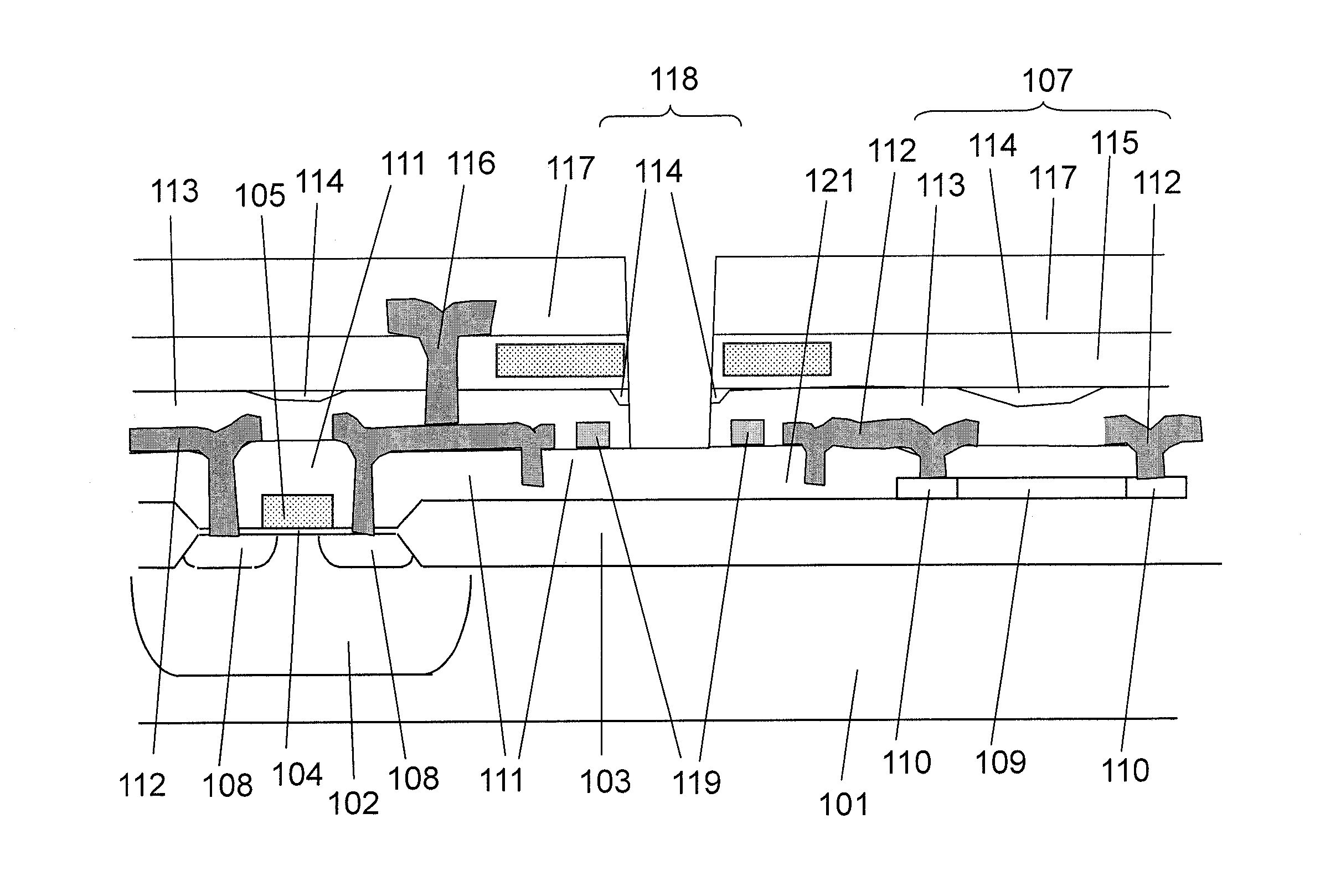
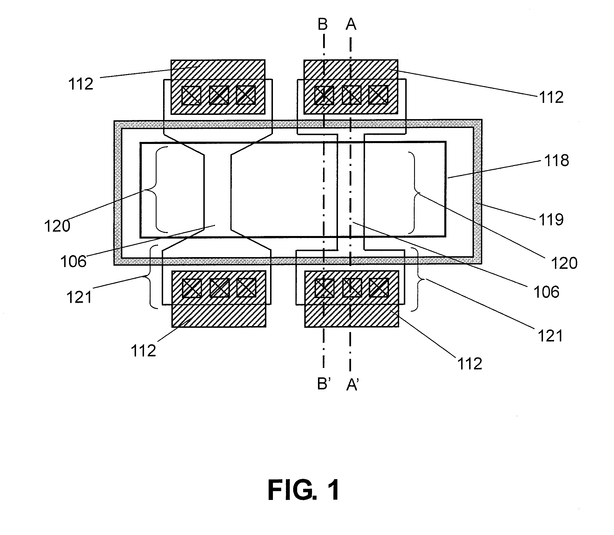
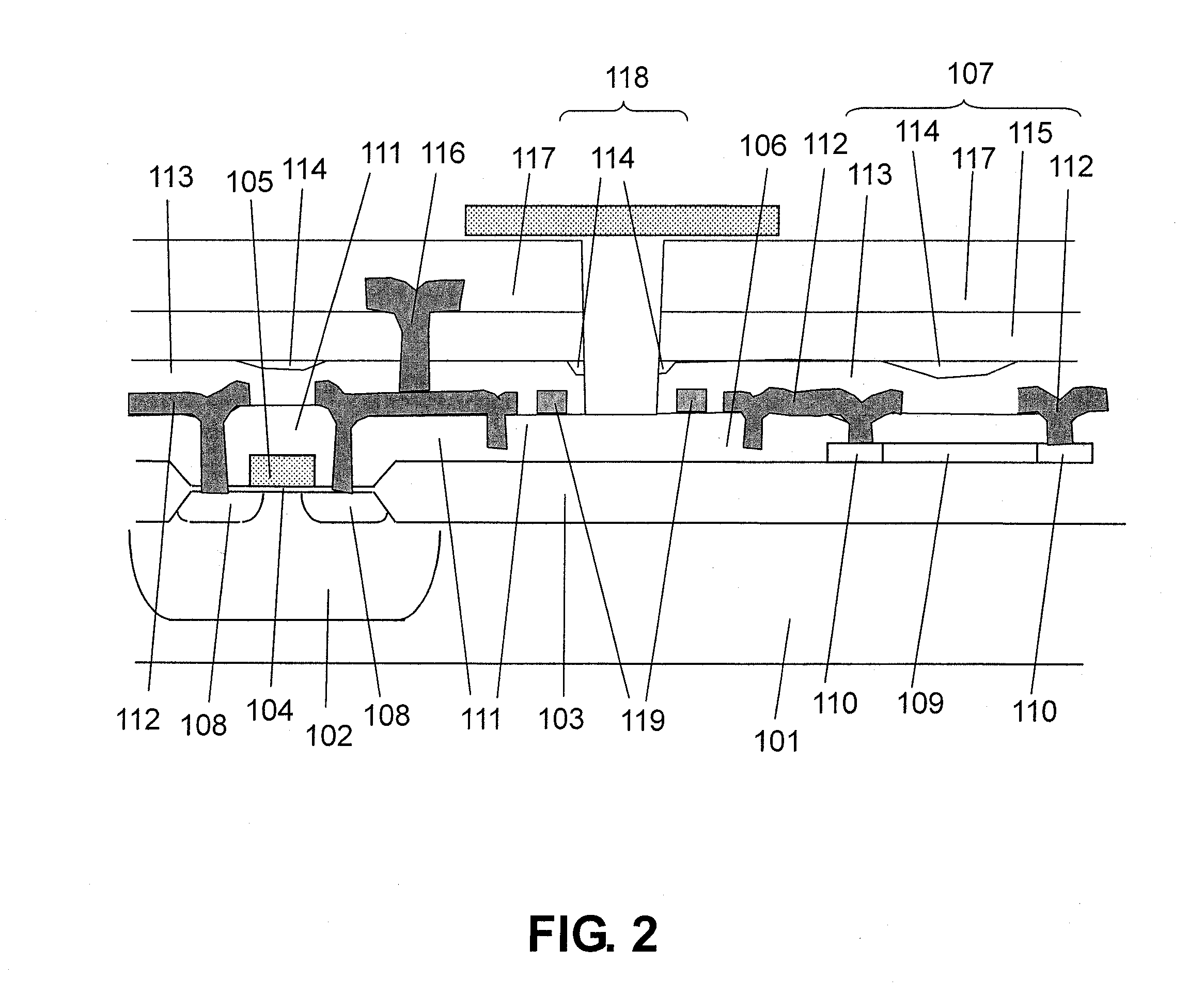
[0026]FIG. 1 illustrates a top view of a fuse portion of a semiconductor device according to the present invention. FIGS. 2 and 3 illustrate schematic cross-sectional views of the semiconductor device according to the present invention.

[0027]It is found from comparison of FIG. 1 with FIG. 4 illustrating the conventional structure that the feature of the semiconductor device of the present invention resides in that a part of a fuse terminal 121 overlaps a part of a seal ring 119 made of a metal wiring layer which is the same as a metal wiring 112. A fuse 106 illustrated on the right side of FIG. 1 has a shape formed of the rectangular fuse terminals 121 and a rectangular fuse trimming laser irradiation portion 120 positioned in a fuse opening portion 118. A fuse 106 illustrated on the left side of FIG. 1 has a shape in which a bonding portion between the fuse terminal 121 and...


PUM


Abstract

Provided is a method of manufacturing a semiconductor device capable of preventing, in a SOG etch back planarization process in a multi-layered wiring process, degradation in long-term reliability with respect to the entering of moisture caused by a fuse opening portion. A fuse is shaped so that polycrystalline silicon extends to a lower part of a guard ring provided in a first layer of metal for preventing the entering of moisture from the fuse opening portion. Thus, a metal wiring used for connection to an electrode of the fuse and a metal wiring of the guard ring become equal in height, and hence an SOG layer can be prevented from reaching the inside of an IC.

Description

RELATED APPLICATIONS[0001]This application claims priority under 35 U.S.C. §119 to Japanese Patent Applications No. 2011-218242 filed on Sep. 30, 2011 and No. 2012-171416 filed on Aug. 1, 2012, the entire content of which is hereby incorporated by reference.BACKGROUND OF THE INVENTION[0002]1. Field of the Invention[0003]The present invention relates to a semiconductor device including a MOS transistor and a resistor.[0004]2. Description of the Related Art[0005]In an analog IC such as a voltage detector, the following measures are typically taken for obtaining desired characteristics for an output voltage. Fuses for laser trimming, which are formed of thin film resistors such as polycrystalline silicon, are disposed, and the fuses are selectively burned and cut by laser irradiation to adjust a combination pattern of the resistors, to thereby adjust fluctuations in characteristics caused by fluctuations at mass production in a wafer process, and adjust a target value of a circuit.[000...

Claims


Application Information

Patent Timeline
IPC IPC(8): H01L23/525
CPCH01L23/5256H01L23/585H01L2924/0002H01L2924/00
Inventor HASEGAWA, HISASHI
Owner ABLIC INC
Why Eureka
Try Eureka