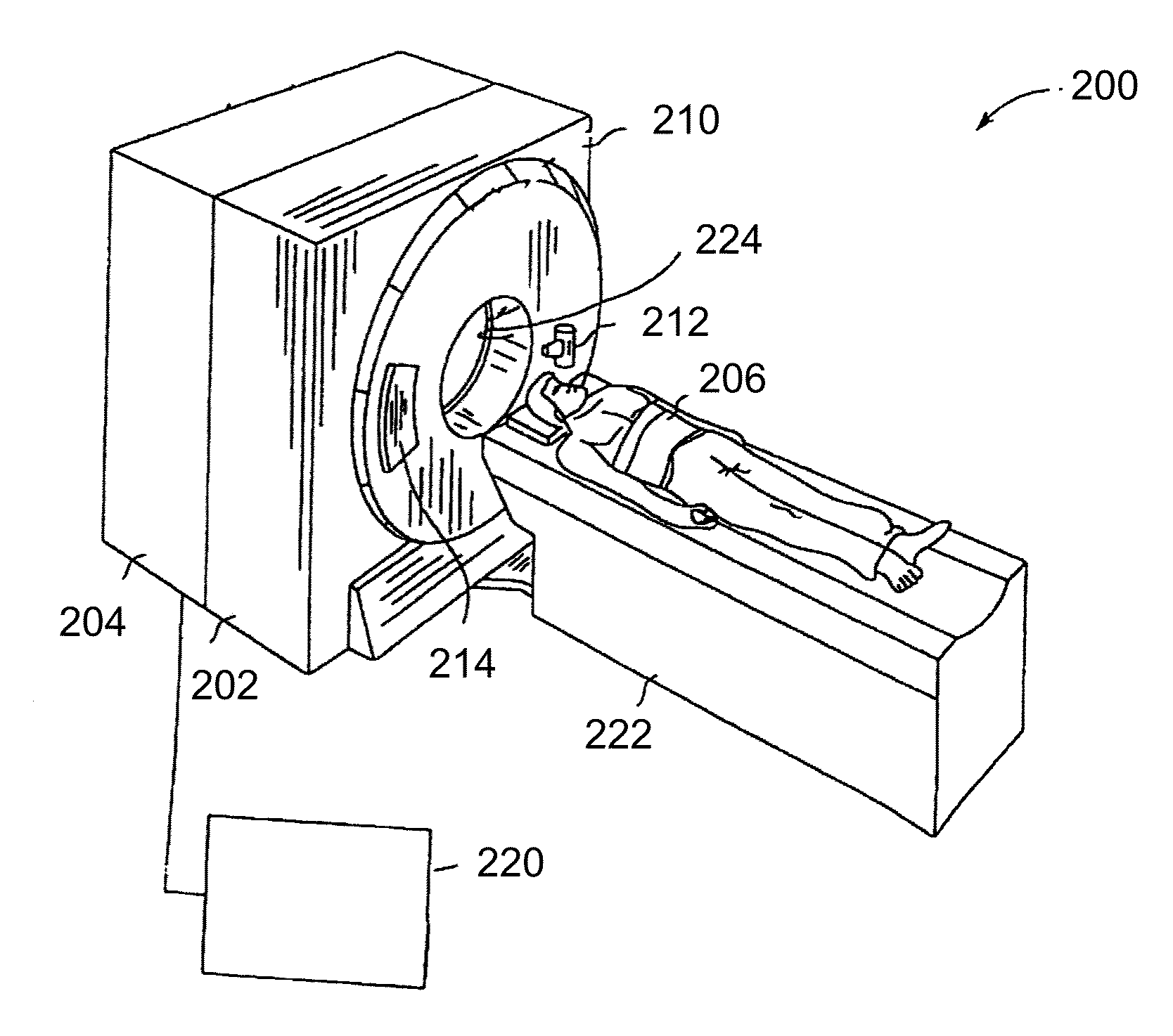
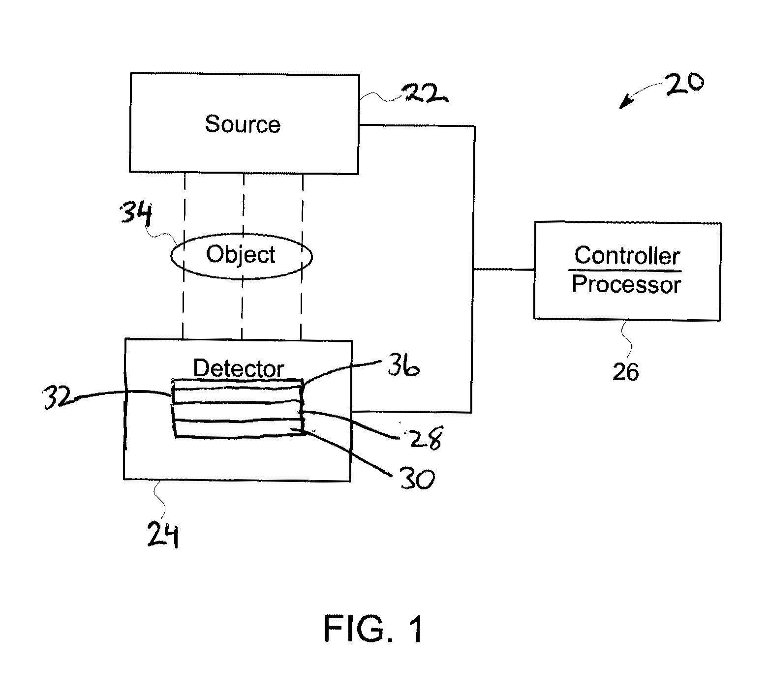
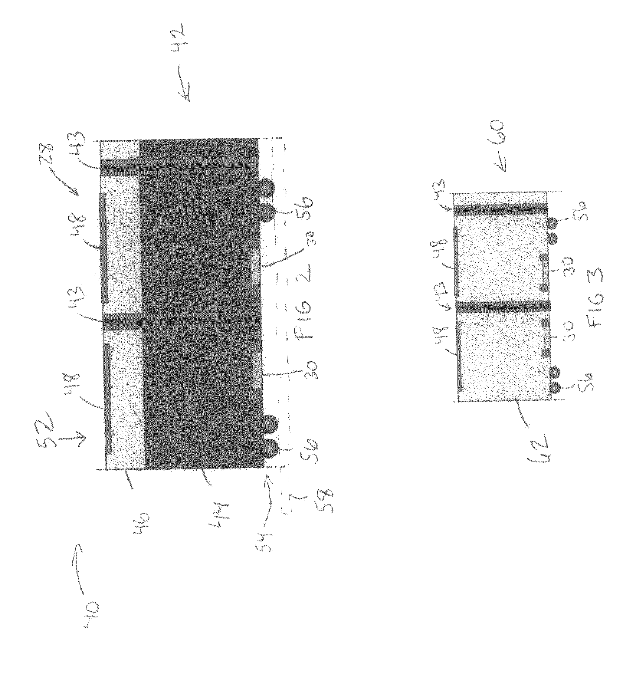
Detector modules and methods of manufacturing

a technology applied in the field of detector modules and manufacturing methods, can solve the problems of increasing the complexity of packaging design to integrate the photosensor array, increasing the risk of interconnection yield and reliability, and complex ceramic substrates that are expensive to manufactur

Active Publication Date: 2013-04-04
GENERAL ELECTRIC CO
View PDF17 Cites 14 Cited by
  • Summary
  • Abstract
  • Description
  • Claims
  • Application Information

AI Technical Summary

Problems solved by technology

Accordingly, the number of analog interconnections between detector pixel arrays and the readout electronics increases, which increases the complexity of the packaging design to integrate the photosensor array and readout electronics including the A / D converter.
For example, some package designs include complex ceramic substrates that are expensive to manufacture.
These ceramics also have increased risk in interconnection yields and reliability.
However, this design results in the loss of the active detection area of the photosensor array and compromises performance as a result of the different requirements on wafer properties for the photosensor and readout electronics.

Method used


Image

  • Detector modules and methods of manufacturing
  • Detector modules and methods of manufacturing
  • Detector modules and methods of manufacturing

Examples


Embodiment Construction

[0016]The following detailed description of certain embodiments will be better understood when read in conjunction with the appended drawings. To the extent that the figures illustrate diagrams of the functional blocks of various embodiments, the functional blocks are not necessarily indicative of the division between hardware circuitry. Thus, for example, one or more of the functional blocks (e.g., processors or memories) may be implemented in a single piece of hardware (e.g., a general purpose signal processor or random access memory, hard disk, or the like) or multiple pieces of hardware. Similarly, the programs may be stand alone programs, may be incorporated as subroutines in an operating system, may be functions in an installed software package, and the like. It should be understood that the various embodiments are not limited to the arrangements and instrumentality shown in the drawings.

[0017]As used herein, an element or step recited in the singular and proceeded with the wo...


PUM


Abstract

Detector modules and methods of manufacturing are provided. One detector module includes a detector having a silicon wafer structure formed from a first layer having a first resistivity and a second layer having a second resistivity, wherein the first resistivity is greater than the second resistivity. The detector further includes a photosensor device provided with the first layer on a first side of the silicon wafer and one or more readout electronics provided with the second layer on a second side of the silicon wafer, with the first side being a different side than the second side.

Description

BACKGROUND[0001]Imaging systems are widely used to capture images of objects. For example, diagnostic images of a person or an animal may be obtained to assist a doctor or other health care professional in making an accurate diagnosis. Another example includes imaging luggage, shipping containers, and / or the like for security and / or industrial inspection applications. Imaging systems often include an energy source and one or more detectors. In particular, energy, for example x-rays, produced by the source travel through the object being imaged and are detected by the detectors. In response thereto, the detectors produce digital signals that represent the sensed energy used for subsequent processing and image reconstruction.[0002]Some imaging systems, such as some computed tomography (CT) imaging systems, continue to increase the number of imaging pixels and the detector coverage. Accordingly, the number of analog interconnections between detector pixel arrays and the readout electro...

Claims


Application Information

Patent Timeline
Patent Type & Authority Applications(United States)
IPC IPC(8): A61B6/03H01L31/18H01L31/02
CPCA61B6/032A61B6/4233A61B6/4266G01T1/242H01L27/14634H01L27/14636H01L31/105H01L27/14676
Inventor LI, WENRAO, NARESH KESAVANIKHLEF, ABDELAZIZKAUTZER, JEFFREY
Owner GENERAL ELECTRIC CO
Why Eureka
Try Eureka