Photon counting cone-beam ct apparatus with monolithic CMOS integrated pixel detectors

a technology of pixel detectors and cone beams, applied in the field of computed tomography (ct) imaging equipment, can solve the problems of limited detection efficiency, reduced radiation dose absorption, and low conversion efficiency of two-stage conversion processes, and achieve the effect of reducing radiation dose absorption

Active Publication Date: 2018-08-23
G RAY SWITZERLAND SA
View PDF2 Cites 13 Cited by
  • Summary
  • Abstract
  • Description
  • Claims
  • Application Information

AI Technical Summary

Benefits of technology

[0030]It is another object of the invention to provide a CBCT with photon counti

Problems solved by technology

Flat-panel detectors (FPD) are widely used for medical imaging and have critically increased safety of minimally invasive and endovascular procedures, however, at the price of increased patient and operator irradiation because of limited detection efficiency.
Apart from limited spatial and energy resolution, the two-stage conversion process suffers from the drawback of low conversion efficiency and limited spectral resolution.
The detective quantum efficiency achievable with polycrystalline and or amorphous semiconductors is, however, again rather low because of their poor electrical transport properties, making FPD derived from such materials ill-suited for interventional radiology.
The list of materials suitable for the fabrication of single crystalline X-ray absorbers is rather limited because they need to have a suitable bandgap and must be of sufficient size and perfection.
On the other hand, its low atomic number Z, makes Si a poor absorber for photon energies above about 20 keV.
It has, however, the drawback of a small bandgap Eg of only 0.66 eV, leading to a resistivity of only 50 Ωkm at room temperature, even when it is undoped and highly pure.
Since, however, large SiGe wafers are not commercially available, one has to resort to epitaxial growth on Si substrates in order to realize FPD based on SiGe.
The large mismatch of lattice parameters and thermal expansion coefficients of Ge and Si cause, however, high defect densities (such as misfit and threading dislocations and stacking faults) and cracks in an epitaxial SiGe layer of sufficient thickness on the order of 100 μm or larger to serve as an X-ray absorber.
In addition, device processing may not be permitted at all due to excessive wafer bowing resulting from the thermal misfit.
The approach does not, however, eliminate the high density of misfit dislocations present at the SiGe/Si interface.
While epitaxial SiGe absorbers can be grown on large wafers at least 200 mm in size, they are necessarily limited in thickness to a range of about 100-200 μm for example for cost reasons.
On the other hand the mobility-lifetime product is much inferior to that of elemental semicond

Method used


Image

  • Photon counting cone-beam ct apparatus with monolithic CMOS integrated pixel detectors
  • Photon counting cone-beam ct apparatus with monolithic CMOS integrated pixel detectors
  • Photon counting cone-beam ct apparatus with monolithic CMOS integrated pixel detectors

Examples


Embodiment Construction

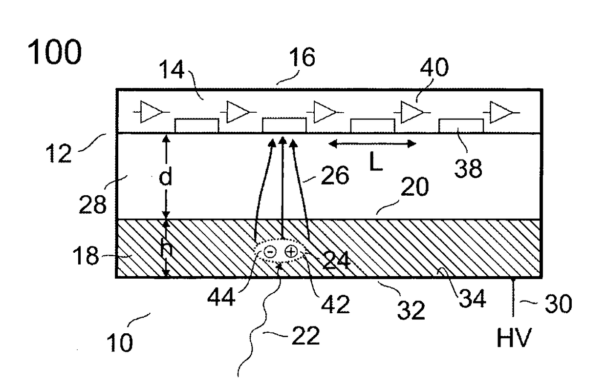
[0072]It is the aim of this invention to enable a multitude of improved capabilities and new applications for X-ray 3D imaging for example in mammography and in the interventional suite at lower radiation dose by overcoming the limits of actual absorption materials in detectors and manufacturing processes.

[0073]The invention solves in particular the problems of materials incompatibility preventing the fabrication of sensitive, large area monolithic pixel detectors (FPD) employing high-Z materials to enhance absorption especially of X-ray photons with energies typically above 40 keV for use for example in C-arm Cone Beam Computed Tomography (CBCT) units. It is based on low-temperature direct wafer bonding techniques, preferably below 100° C. or even at room temperature, by means of which a CMOS processed readout unit and a single crystal absorber are combined in a monolithic detector structure. The invention is applicable in principle to any absorber material of which large wafers co...


PUM


Abstract

CBCT including monolithic photon counting FPD for medical applications requiring real-time 3D imaging, like mammography, interventional guided procedures or external beam radiotherapy, includes CMOS processed readout electronics monolithically integrated with a single crystalline X-ray absorber by covalent wafer bonding near room temperature and adapted for single photon counting providing high energy, temporal and spatial resolution.

Description

CROSS REFERENCE TO RELATED APPLICATIONS[0001]This application claims priority to and benefits of PCT application no. PCT / IB2015 / 002385, filed Dec. 21, 2015 and U.S. Provisional Application No. 62 / 211,958, filed 31 Aug. 2015, the contents of which are incorporated herein by reference hereto and relied upon; this application further claims priority to U.S. Provisional Application No. 62 / 295,720, filed Feb. 16, 2016, the contents of which are incorporated herein by reference hereto and relied upon.FIELD OF THE INVENTION[0002]The invention relates to computed tomography (CT) imaging equipment and more specifically to cone beam computer tomography (CBCT) with monolithically integrated semiconductor detectors with energy discriminating capabilities.BACKGROUND OF THE INVENTION[0003]Many medical applications requiring 3D real-time X-ray imaging, like angiographic interventions including vascular stent and stent graft placements, transcatheter embolization and targeted intravascular oncologi...

Claims


Application Information

Patent Timeline
IPC IPC(8): H01L27/146A61B6/00A61B6/03H01L23/00
CPCH01L27/14661A61B6/4085A61B6/03A61B6/4241A61B6/4441H01L27/14634H01L27/14689H01L27/1469A61B6/502A61B6/504H01L24/16A61B6/032H01L27/14636A61B6/4233H01L27/14659G01T1/00
Inventor MEYLAN, CLAUDEVON KANEL, HANS
Owner G RAY SWITZERLAND SA
Why Eureka
Try Eureka