Solid-state imaging apparatus

Inactive Publication Date: 2013-04-11
CANON KK
View PDF4 Cites 4 Cited by
  • Summary
  • Abstract
  • Description
  • Claims
  • Application Information

AI Technical Summary

Benefits of technology

The patent text is discussing a way to make smaller circuitry for reading columns of data. When the size of the circuit is reduced, the text explains that two capacitances in the circuit can be large, which makes it necessary to decrease the capacitance to make the circuit smaller. By doing this, the text says that the offset for charge injection caused by a MOS switch is increased, which can improve the performance of the circuit.

Problems solved by technology

When the number of the column reading circuits is increased, increase in the delay differences among the control signals due to increased load may become a problem.
The present inventor found that, when the pitches in the reading circuit are narrowed, the offset of the gain amplifier may not be sufficiently reduced by the differential amplifier.
If the offset of the gain amplifier may not be sufficiently removed by the differential amplifier or a processing device provided outside of the solid-state imaging apparatus, an image signal in which a fixed pattern noise remains is output, so that quality of the acquired image may deteriorate.

Method used


Image

  • Solid-state imaging apparatus
  • Solid-state imaging apparatus
  • Solid-state imaging apparatus

Examples


Embodiment Construction

[0024]Various exemplary embodiments, features, and aspects of the embodiments will be described in detail below with reference to the drawings. One disclosed feature of the embodiments may be described as a process which is usually depicted as a timing diagram. A timing diagram may illustrate the timing relationships of several entities, such as signals, events, etc. Although a timing diagram may describe the operations as a sequential process, some operations may be performed in parallel or concurrently. In addition, unless specifically stated, the order of the operations or timing instants may be re-arranged. Furthermore, the timing or temporal distances may not be scaled or depict the timing relationships in exact proportions.

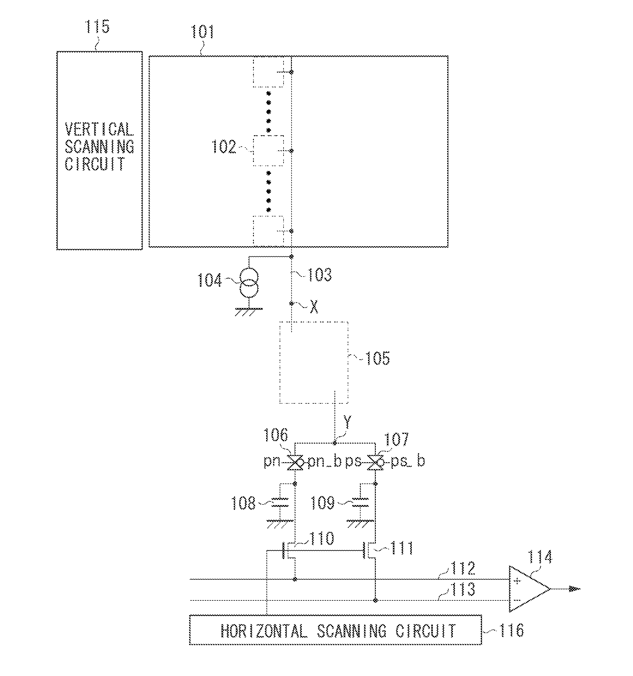
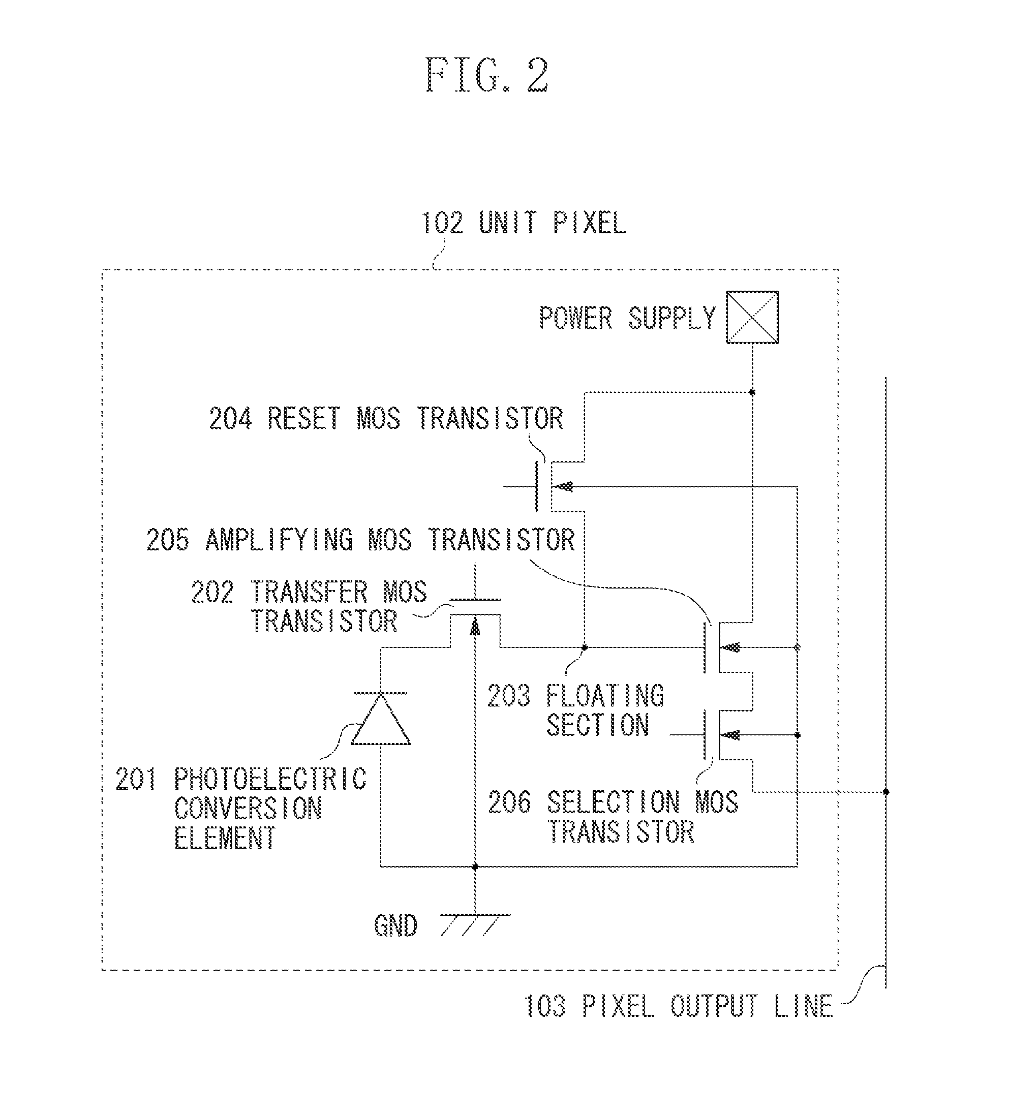
[0025]FIG. 1 illustrates an example of a configuration of a solid-state imaging apparatus according to a first exemplary embodiment. A pixel region 101 is arranged in a two-dimensional matrix, and includes a plurality of unit pixels 102 for generating a sign...


PUM


Abstract

An imaging apparatus includes a plurality of unit pixels arranged in a matrix and configured to generate a signal by photoelectric conversion, a plurality of pixel output lines connected to each column of the unit pixels, a plurality of column amplifiers configured to amplify a signal of the pixel output lines, and a driving circuit configured to generate a control signal of the column amplifiers. Each of the column amplifiers includes first and second input terminals, an output terminal, an input capacitance between the first and second input terminals, and a first switch between the second input and output terminals. The driving circuit is configured to generate the control signal so as to make a period for switching the first switch from a conductive state to a non-conductive state longer than a period for switching the first switch from the non-conductive state to the conductive state.

Description

BACKGROUND OF THE INVENTION[0001]1. Field of the Invention[0002]One disclosed aspect of the embodiments relates to a solid-state imaging apparatus.[0003]2. Description of the Related Art[0004]Japanese Patent Application Laid-Open No. 2003-51989 discusses a technique for amplifying signals output from pixels of each column in a pixel array in which a plurality of pixels is two-dimensionally arranged, by a gain amplifier of each column. As a configuration of the gain amplifier for the each column, a capacitive feedback type inverting amplifier is described. When a metal-oxide semiconductor (MOS) switch provided at a feedback path is conductive, the gain amplifier is operated as a voltage follower to initialize an inverting input unit. Further, Japanese Patent Application Laid-Open No. 2003-51989 discusses a technique for reducing offset of each gain amplifier using a differential amplifier commonly provided for a plurality of gain amplifiers.[0005]In recent years, demands for solid-st...

Claims


Application Information

Patent Timeline
IPC IPC(8): H01L27/148
CPCH04N5/3572H04N5/378H04N5/3742H04N5/365H04N25/67H04N25/767H04N25/75
Inventor ITANO, TETSUYAHIYAMA, HIROKISAITO, KAZUHIRONAKAMURA, KOHICHIIWATA, KOICHIROMAEHASHI, YUAKIYAMA, TAKESHI
Owner CANON KK
Why Eureka
Try Eureka