Semiconductor structures and fabrication method

Active Publication Date: 2013-05-02
SHANGHAI HUAHONG GRACE SEMICON MFG CORP
View PDF2 Cites 30 Cited by
  • Summary
  • Abstract
  • Description
  • Claims
  • Application Information

AI Technical Summary

Problems solved by technology

Therefore, the width, doping concentration and inner defects of the N drift region can significantly affect the device performance.
Similarly, voltage tolerance and surface breakdown of P—N junction may also significantly affect the device performance.
Thus, there is a limitation concerning the dependence of on-resistance on breakdown voltage, called “silicon limit”, under which on-resistance cannot be lowered further.
Although SJMOSFETs have great advantages compared to conventional MOSFETs, the fabrication process is difficult due to the difficulties for forming alternatively distributed P-type and N-type semiconductor regions.
The first method is easier than the second one, but with a higher

Method used


Image

  • Semiconductor structures and fabrication method
  • Semiconductor structures and fabrication method
  • Semiconductor structures and fabrication method

Examples


Embodiment Construction

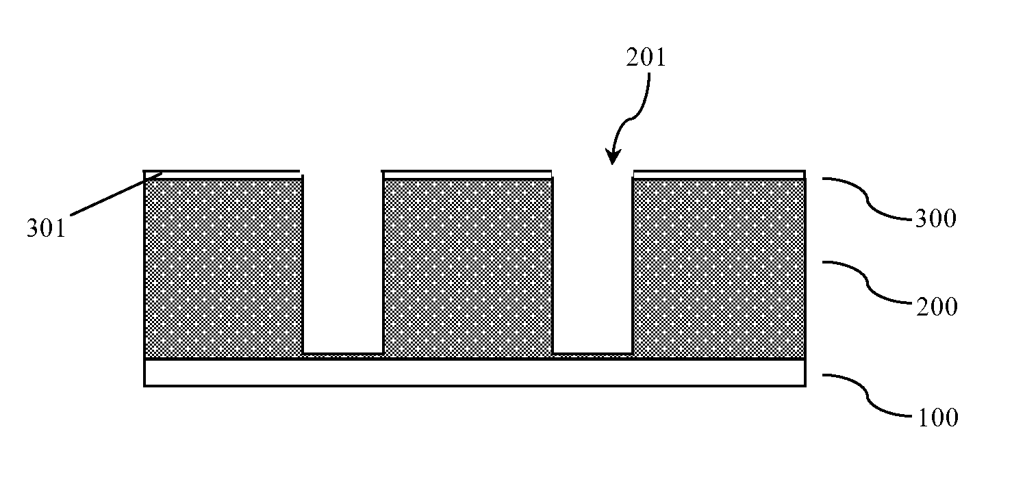
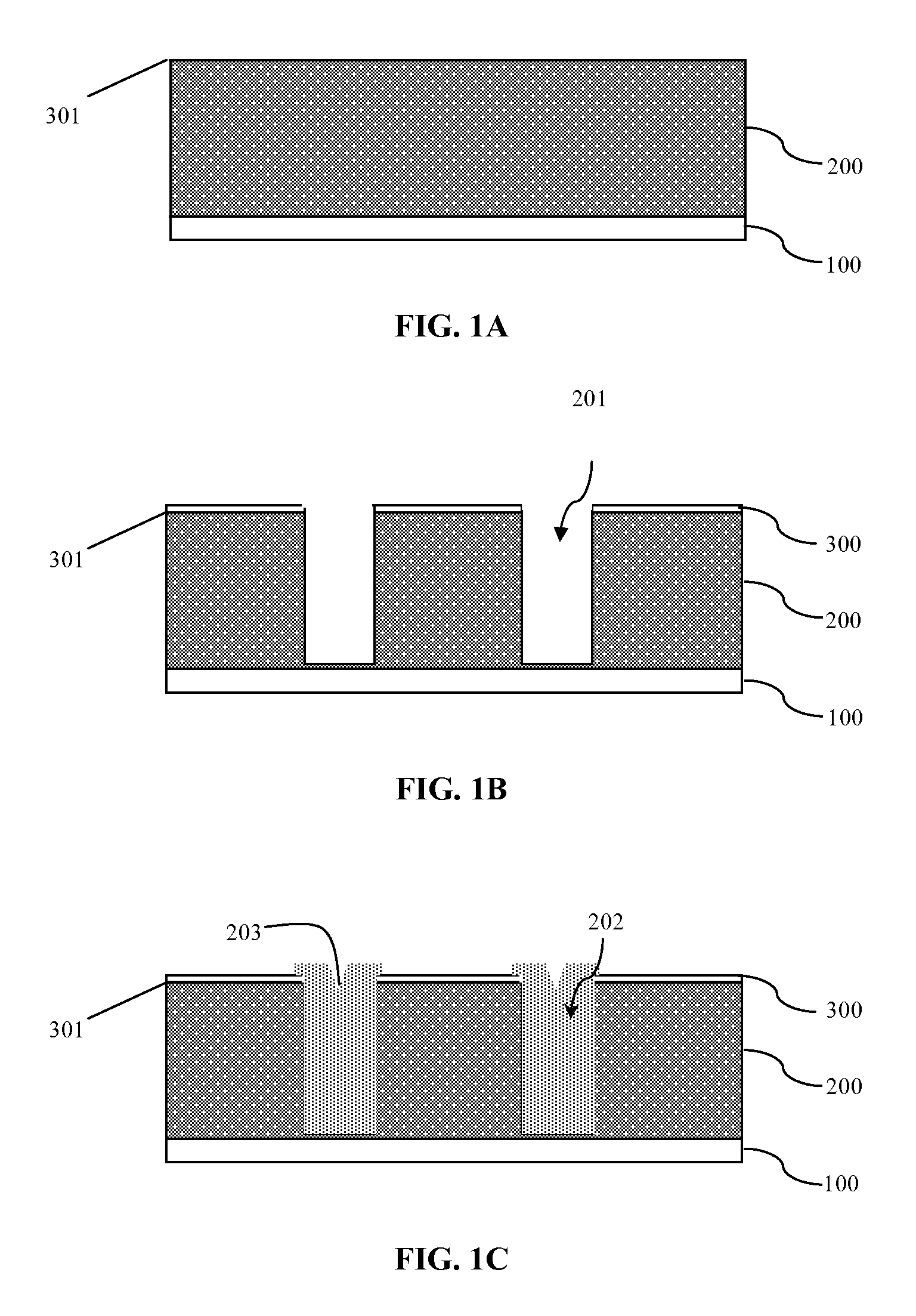
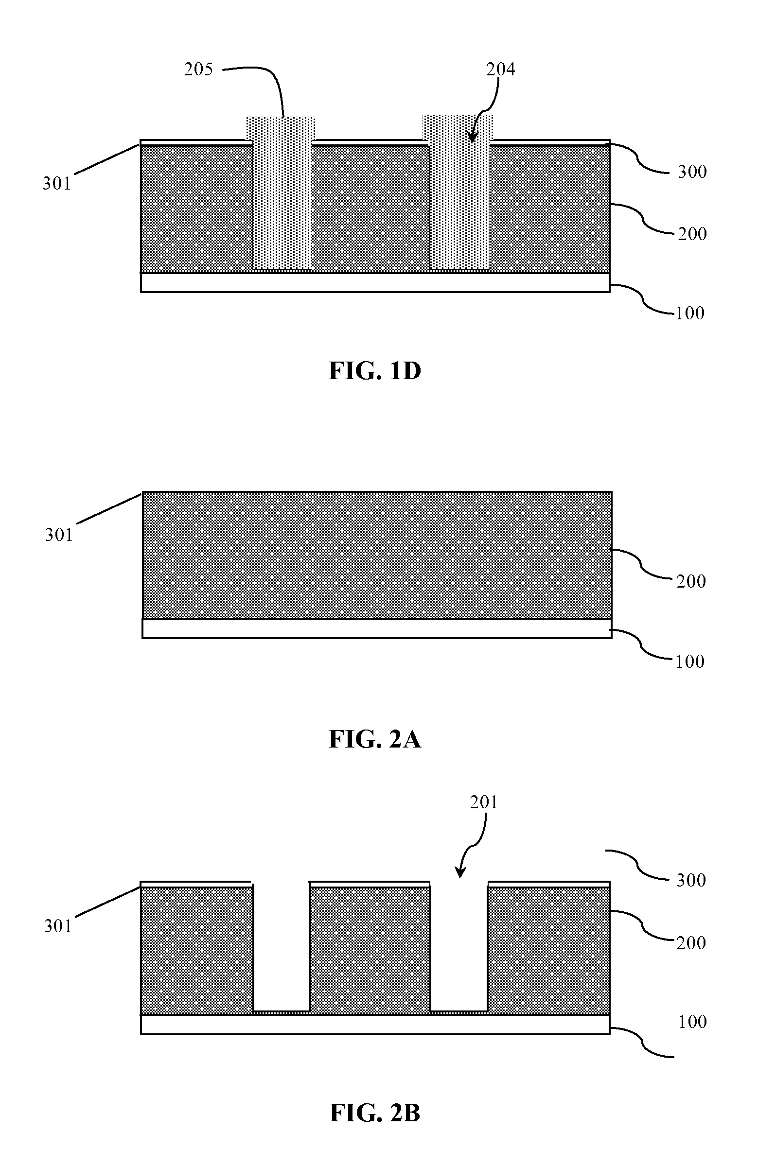
[0039]Reference will now be made in detail to exemplary embodiments of the invention, which are illustrated in the accompanying drawings. Wherever possible, the same reference numbers will be used throughout the drawings to refer to the same or like parts.

[0040]Certain terms and / or definitions are explained first. The term on-resistance (RON), as used herein, may refer to the resistance that exists when a semiconductor device overcomes the semiconducting characteristics to become electrically conductive, which is closely related to the doping level of the semiconductor device.

[0041]The term breakdown voltage (VBD), as used herein, may refer to the minimum voltage that cause portion of an insulator to become electrically conductive. That is, the insulator will lost its dielectric properties and change from semiconductor to conductor at or above the minimum voltage, which is called breakdown, and the corresponding minimum voltage is called breakdown voltage.

[0042]The term reduced pres...


PUM

PropertyMeasurementUnit
Angleaaaaaaaaaa
Flow rateaaaaaaaaaa
Widthaaaaaaaaaa

Abstract

A method is provided for fabricating a semiconductor structure. The method includes providing a semiconductor substrate, forming an epitaxial layer on a top surface of the semiconductor substrate and having a predetermined thickness, and forming a plurality of trenches in the epitaxial layer. The trenches are formed in the epitaxial layer and have a predetermined depth, top width, and bottom width. Further, the method includes performing a first trench filling process to form a semiconductor layer inside of the trenches using a mixture gas containing at least silicon source gas and halogenoid gas, stopping the first trench filling process when at least one trench is not completely filled, and performing a second trench filling process, different from the first trench filling process, to fill the plurality of trenches completely.

Description

CROSS-REFERENCES TO RELATED APPLICATIONS[0001]This application claims the priority of Chinese patent application No. 201110337812.1, filed on Oct. 31, 2011, the entirety of which is incorporated herein by reference.FIELD OF THE INVENTION[0002]The present invention generally relates to the field of semiconductor manufacturing technology and, more particularly, relates to techniques for fabricating high-performance semiconductor devices utilizing silicon epitaxial growth trench filling methods.BACKGROUND[0003]It is well known that power semiconductor devices are the building blocks of power electronic products, which have been developed rapidly due to the intensive demands in the recent years. With the development of semiconductor technology, the size of power semiconductor devices continues to shrink; their weights become lighter; the safety and reliability of these devices are higher; and the power consumption is lower. Power semiconductor devices, also called power electronic devic...

Claims


Application Information

Patent Timeline
IPC IPC(8): H01L29/04H01L21/20
CPCH01L21/02532H01L21/02576H01L21/02639H01L21/0262H01L21/02579
Inventor LIU, JIQUANXIAO, SHENGANJI, WEI
Owner SHANGHAI HUAHONG GRACE SEMICON MFG CORP
Why Eureka
Try Eureka