Microlens array and optical transmission component

a microlens array and optical transmission technology, applied in the field of microlens array and optical transmission components, can solve the problems of difficult cost reduction, insufficient accuracy of the lens center position coinciding with the waveguide center, etc., and achieve the effects of high accuracy, easy connection, and convenient manufacturing

Active Publication Date: 2013-05-02
NTT ELECTORNICS CORP +1
View PDF1 Cites 1 Cited by
  • Summary
  • Abstract
  • Description
  • Claims
  • Application Information

AI Technical Summary

Benefits of technology

[0018]In the optical circuit, a waveguide for alignment is formed so as to be in parallel with a waveguide for a signal. Since positional alignment between the waveguide for alignment and the fiber for alignment of the microlens array can be easily performed, the microlens and the waveguide of the optical circuit can be easily connected with high accuracy.
[0019]Accordingly, the present disclosure can provide an optical transmission component easily manufactured while securing high connection accuracy between the optical circuit such as a waveguide and the microlens array.
[0020]The present disclosure can provide a microlens array which maintains high positional accuracy with respect to an optical circuit such as a waveguide and facilitates connection operation, and an optical transmission component including the microlens array.

Problems solved by technology

Namely, a position-monitoring light intensity curve shown in a duplex manner at the right end in FIG. 3B is in a trapezoidal shape, and the lens center position coinciding with the waveguide center is not obtained with sufficient accuracy.
Thus, the above method has a problem that a lens mounting operation is complex, including provision of a dedicated device specifically for an optical circuit-lens connection process and it is difficult to reduce cost.

Method used


Image

  • Microlens array and optical transmission component
  • Microlens array and optical transmission component
  • Microlens array and optical transmission component

Examples


embodiment

EFFECT OF EMBODIMENT

[0042]As described above, according to the present embodiment, the following effects can be expected.

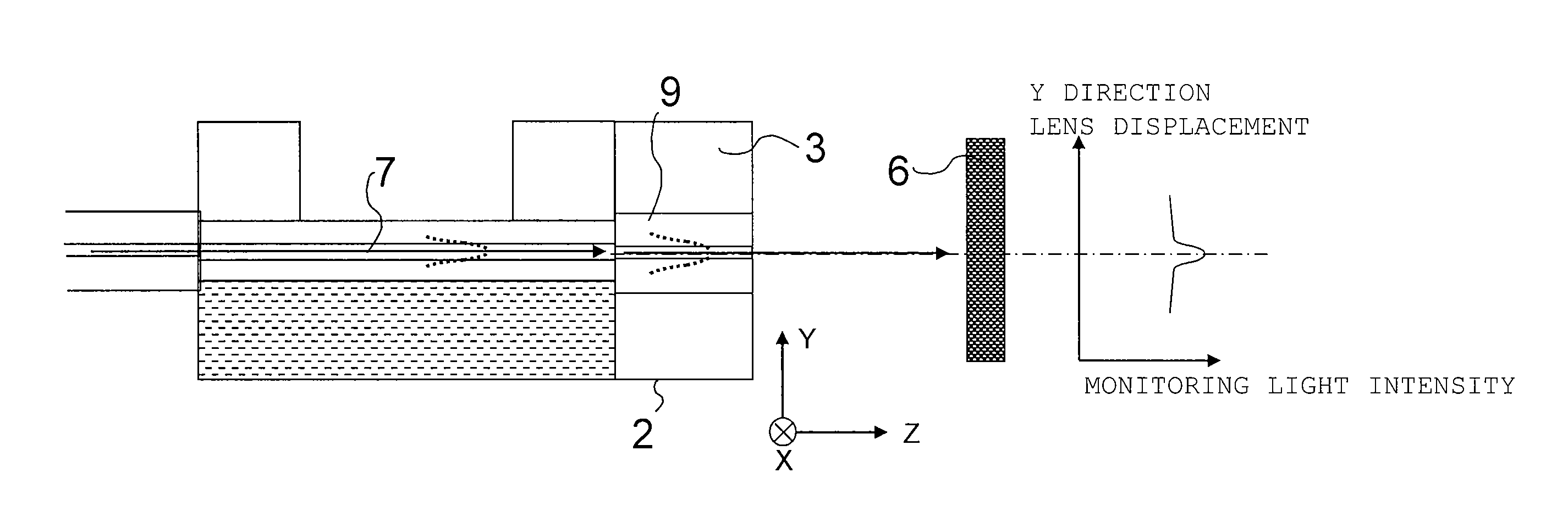
[0043]First, in the present embodiment, the optical fiber for alignments 9 are provided on the both sides of the array of the microlens 1, and the corresponding optical fibers 11 are provided on the input side of the optical circuit. However, the outer diameter accuracy of the optical fiber 11 is held within ±1 μm; moreover, the cost of the optical fiber is low, and a multi-array technique in a fiber block manufacture technique utilizing a V-shaped groove progresses. Thus, there is no technical difficulty.

[0044]Although the waveguide for alignment 10 is required to be provided in the optical circuit 5, the waveguide for alignment 10 is just used for the alignment operation, and the waveguide for alignment 10 is just provided on a photomask at the stage of designing regardless of the quality of the waveguide itself.

[0045]Accordingly, application of this structure h...


PUM


Abstract

A microlens array, which maintains high positional accuracy with respect to an optical circuit such as a waveguide and facilitates connection operation, and an optical transmission component including the microlens array.
Solution
The microlens array is provided with a plurality of microlenses arranged in an array structure and having the same length in the optical axis direction and optical fibers for alignment arranged at both ends of the array structure so that the optical axis is parallel to the optical axis of the microlens and having a length in the optical axis direction the same as the length of the microlens and a guided mode diameter smaller than an aperture of the microlens.

Description

BACKGROUND[0001]1. Field of the Disclosure[0002]The present disclosure relates to a microlens array, which interconnects a planar lightwave circuit and array of optical semiconductor element such as a photodiode used in an optical communication field, and an optical transmission component including the microlens array.[0003]2. Discussion of the Background Art[0004]A gradient index (hereinafter referred to as GI) multimode optical fiber used in optical communication has a square refractive index distribution in which the refractive index is maximum at the core center and exhibits a good lens function when the optical fiber is used as not only an optical transmission path as a primary role but a microlens. Thus, the optical fiber is used for optical coupling between an optical circuit and an optical semiconductor element such as a photodiode (hereinafter referred to as PD).[0005]FIG. 1 is an example of a conventional type of microlens array used for such an object (for example, see Pa...

Claims


Application Information

Patent Timeline
Patent Type & Authority Applications(United States)
IPC IPC(8): G02B6/32
CPCG02B6/3636G02B6/423G02B6/4204G02B3/005G02B3/0025
Inventor TERUI, HIROSHIEBISAWA, FUMIHIROSOMA, SHUNICHIKOMIYAMA, AKIRAMORITA, KEIICHINAKAJIMA, FUMITONASU, YUSUKE
Owner NTT ELECTORNICS CORP
Why Eureka
Try Eureka