Light-emitting device and manufacturing method therefor

Active Publication Date: 2013-05-16
SHARP KK
View PDF1 Cites 20 Cited by
  • Summary
  • Abstract
  • Description
  • Claims
  • Application Information

AI Technical Summary

Benefits of technology

[0052]In addition, due to the presence of the reinforcement material, conductive minute dust and the like can be prevented from entering into the above gap, and short circuit between the pair of the terminal portions can be prevented. Also, when the reinforcement material is slightly projected downward from the bottom surface of the terminal portion, the projection becomes a jett

Problems solved by technology

Therefore, in order to cut out and use the required number of the light-emitting devices from the flexible wiring substrate, it is necessary to cut the flexible wiring substrate by a special processing device, thus this structure is not considered as appropriate for mass production at a low cost.
In order to cut out and use the required number of the light-emitting devices, it is necessary to cut a substrate

Method used


Image

  • Light-emitting device and manufacturing method therefor
  • Light-emitting device and manufacturing method therefor
  • Light-emitting device and manufacturing method therefor

Examples


second embodiment

[0088]FIGS. 9A to 9C schematically show a perspective view (FIG. 9A), a side view viewed from the Y direction (FIG. 9B), and a bottom view viewed from the bottom side (FIG. 9C) of a light-emitting device 13 of the second embodiment, respectively.

[0089]The light-emitting device 13 of the second embodiment is different from the light-emitting device 1 described in the first embodiment in the following two points. First, it is different in that a reinforcement material 14 is filled in a gap between a pair of the terminal portions 4a and 4b in one unit section. Second, a method of injecting the silicon resin 26 into the openings 23 of the metal mask 24 described in FIG. 5A is different. Since the light-emitting device 13 is same as the light-emitting device 1 described in the first embodiment other than the above two differences, a duplicate description is omitted.

first embodiment

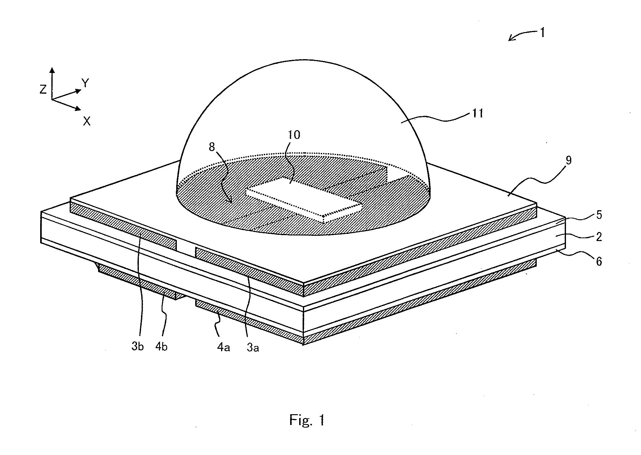
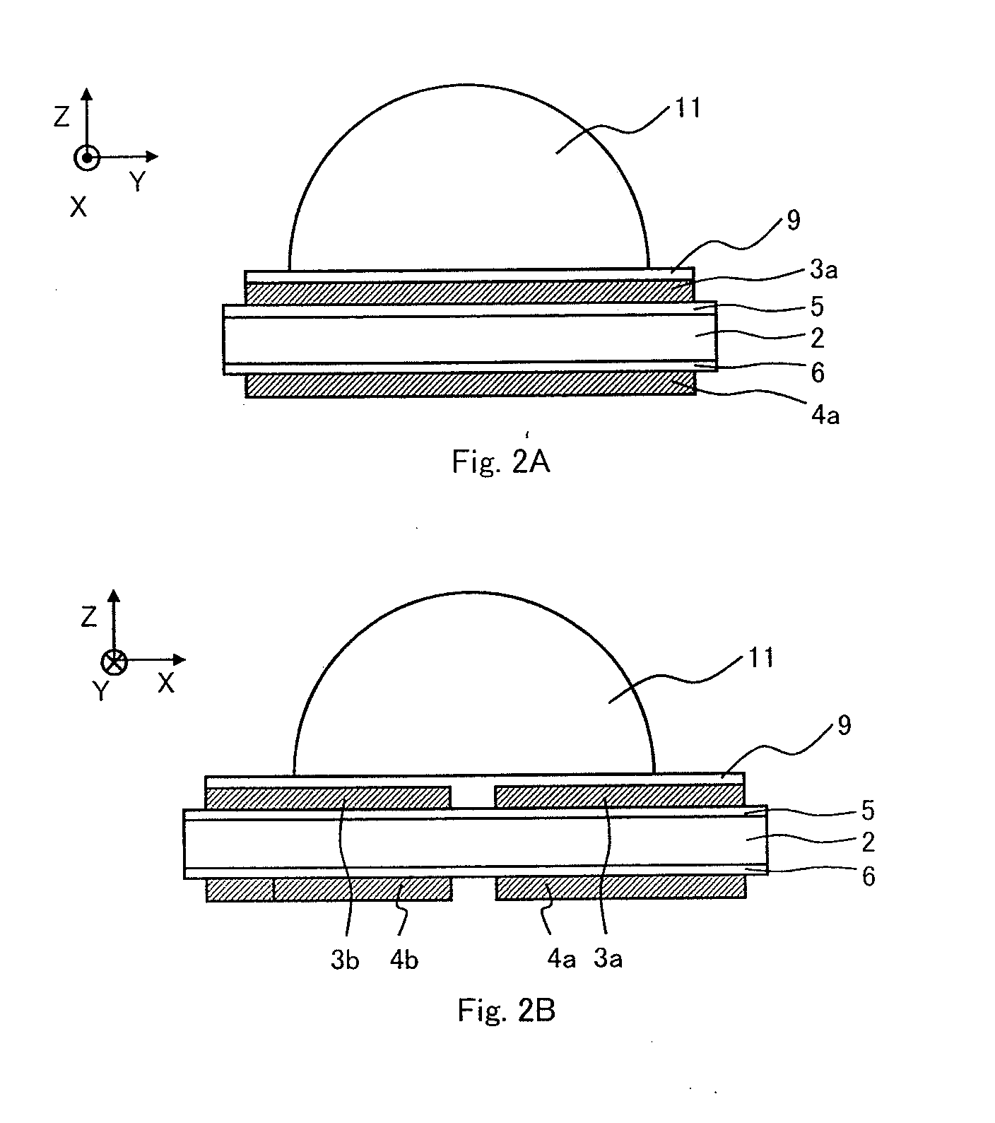
[0090]First, the reinforcement material 14 will be described. The laminate substrate in which the land portions 3a and 3b and the terminal portions 4a and 4b are formed on the both surfaces of the insulating film 2 requires reinforcement since only the insulating film 2 is present between the land portions 3a and 3b and between the terminal portions 4a and 4b. In the first embodiment, the liquid-repellent layer 9 is formed on the land portions 3a and 3b, and the light-emitting element 10 is die-bonded across the land portions 3a and 3b in the opening 8, and a part of the liquid-repellent layer 9 and a part of the silicon resin 11 are filled into the gap between the land portions 3a and 3b. Therefore, a certain level of reinforcement is made in the top side of the insulating film 2. However, since the gap between the terminal portions 4a and 4b remains to be present in the bottom side of the insulating film 2, further reinforcement is possible.

[0091]Therefore, in the second embodimen...

third embodiment

[0098]FIGS. 11A to 11C schematically show a perspective view (FIG. 11A), a side view viewed from the Y direction (FIG. 11B), and a bottom view viewed from the bottom side (FIG. 11C) of a light-emitting device 15 of the third embodiment, respectively.

[0099]The light-emitting device 15 of the third embodiment is different from the light-emitting device 1 described in the first embodiment in the following four points. First, it is different in that a reinforcement material 14 is filled in a gap between a pair of the terminal portions 4a and 4b in one unit section. Second, it is different in that the liquid-repellent layer 9 contains phosphor. Third, it is different in that a wire-bonding type light-emitting element having bonding pads of a P electrode (anode) 10a and an N electrode (cathode) 10b on the chip front surface side, emitting light from the front surface side, and having an insulating substrate such as sapphire on the back surface side is used as a light-emitting element 10, ...


PUM


Abstract

A low-cost and productivity-oriented surface mount light-emitting device is provided. The light-emitting device includes an insulating film 2, at least one pair of land portions 3a and 3b comprising metal film pieces formed on the top surface of the insulating film 2, external connection terminal portions 4a and 4b comprising metal film pieces formed on the bottom surface of the insulating film 2, that are opposed to the land portions 3a and 3b across the insulating film 2 in one-to-one correspondence, through-conductors 7a and 7b that connect between the land portions 3a and 3b and the terminal portions 4a and 4b corresponding to each other through the insulating film 2, and a light-emitting element 10 that is electrically connected to the pair of the land portions 3a and 3b and disposed in a unit section which contains the pair of the land portions 3a and 3b.

Description

REFERENCE TO RELATED APPLICATIONS[0001]This application is a national stage application under 35 USC 371 of International Application No. PCT / JP2011 / 064624, filed Jun. 27, 2011, which claims the priority of Japanese Patent Application No. 2010-166415, filed Jul. 23, 2010, the entire contents of which are incorporated herein by reference.FIELD OF THE INVENTION[0002]The present invention relates to a surface mount light-emitting device and a manufacturing method therefor, and particularly relates to a low-cost and productivity-oriented surface mount light-emitting device and a manufacturing method therefor.BACKGROUND OF THE INVENTION[0003]As a surface mount light-emitting device in which a dice of a light-emitting diode (LED) (semiconductor bare chip) is mounted on a substrate surface and sealed with a transparent resin, for example, there are those disclosed in Patent Document 1 and Patent Document 2 described below, and the like.[0004]An example of a cross-sectional constitution of ...

Claims


Application Information

Patent Timeline
IPC IPC(8): H01L33/62H01L33/50
CPCH01L33/486H01L33/62H01L2933/0033H01L2933/005H01L2224/16225H01L2224/48227H01L2224/73265H01L2224/32225H01L33/50H01L2933/0041H01L2924/00
Inventor KATOH, MASAAKIHATA, TOSHIO
Owner SHARP KK
Why Eureka
Try Eureka