Semiconductor device and method for fabricating the same

a technology of semiconductors and semiconductors, applied in the direction of semiconductor devices, basic electric elements, electrical equipment, etc., can solve the problems of abnormal operation of electronic products, damage to most electronic devices or systems, and affect the circuit functions of integrated circuits (ics), so as to improve esd performance, facilitate fabrication, and induce punch-through currents.

Active Publication Date: 2013-05-23
MARLIN SEMICON LTD
View PDF5 Cites 50 Cited by
  • Summary
  • Abstract
  • Description
  • Claims
  • Application Information

AI Technical Summary

Benefits of technology

[0019]As mentioned above, in the semiconductor device and the method for fabricating the same of the present invention, the proposed doped regions can induce punch-through currents more easily at respective junctions, so as to provide possible current leakage paths for ESD purposes. Besides, the fabricating method is entirely compatible with the current FinFET process, such that the fabrication is simple and the ESD performance can be improved.

Problems solved by technology

ESD is the main factor of electrical overstress (EOS) which causes damage to most of electronic devices or systems.
Such damage can result in the permanent damage of semiconductor devices and computer systems, so that circuit functions of integrated circuits (ICs) are affected and operation of electronic products is abnormal.

Method used


Image

  • Semiconductor device and method for fabricating the same
  • Semiconductor device and method for fabricating the same
  • Semiconductor device and method for fabricating the same

Examples


Embodiment Construction

[0025]Reference will now be made in detail to the present preferred embodiments of the invention, examples of which are illustrated in the accompanying drawings. Wherever possible, the same reference numbers are used in the drawings and the description to refer to the same or like parts.

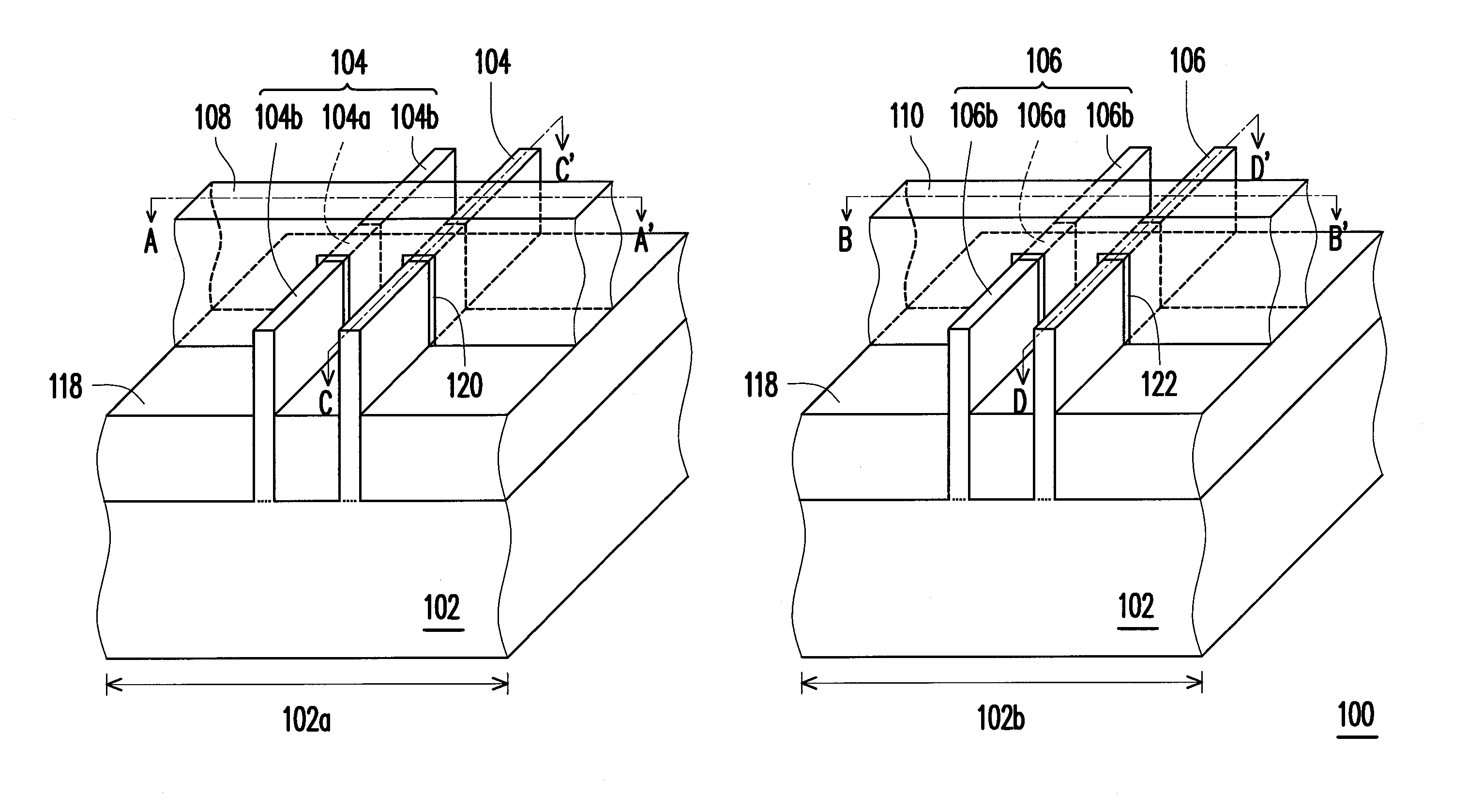
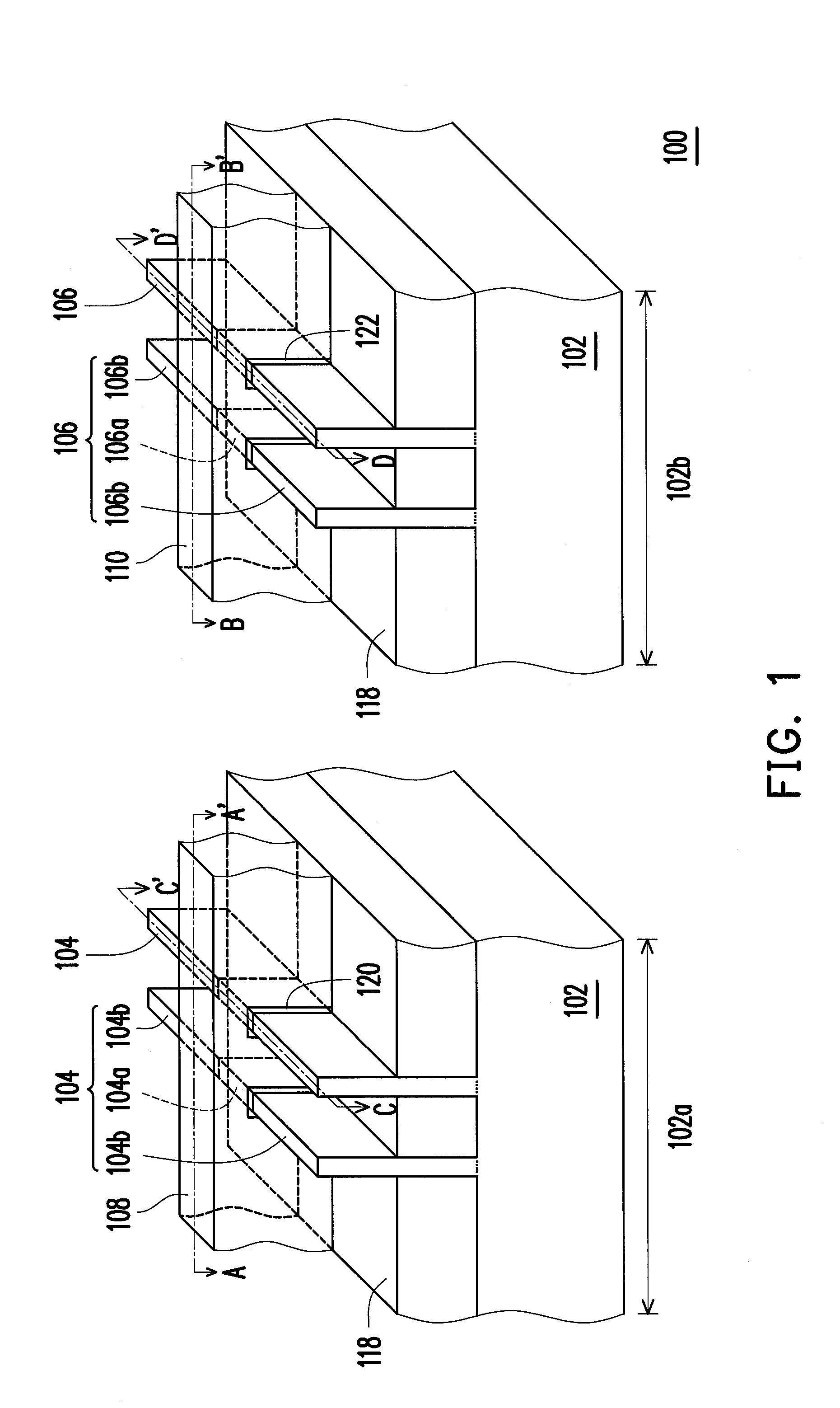
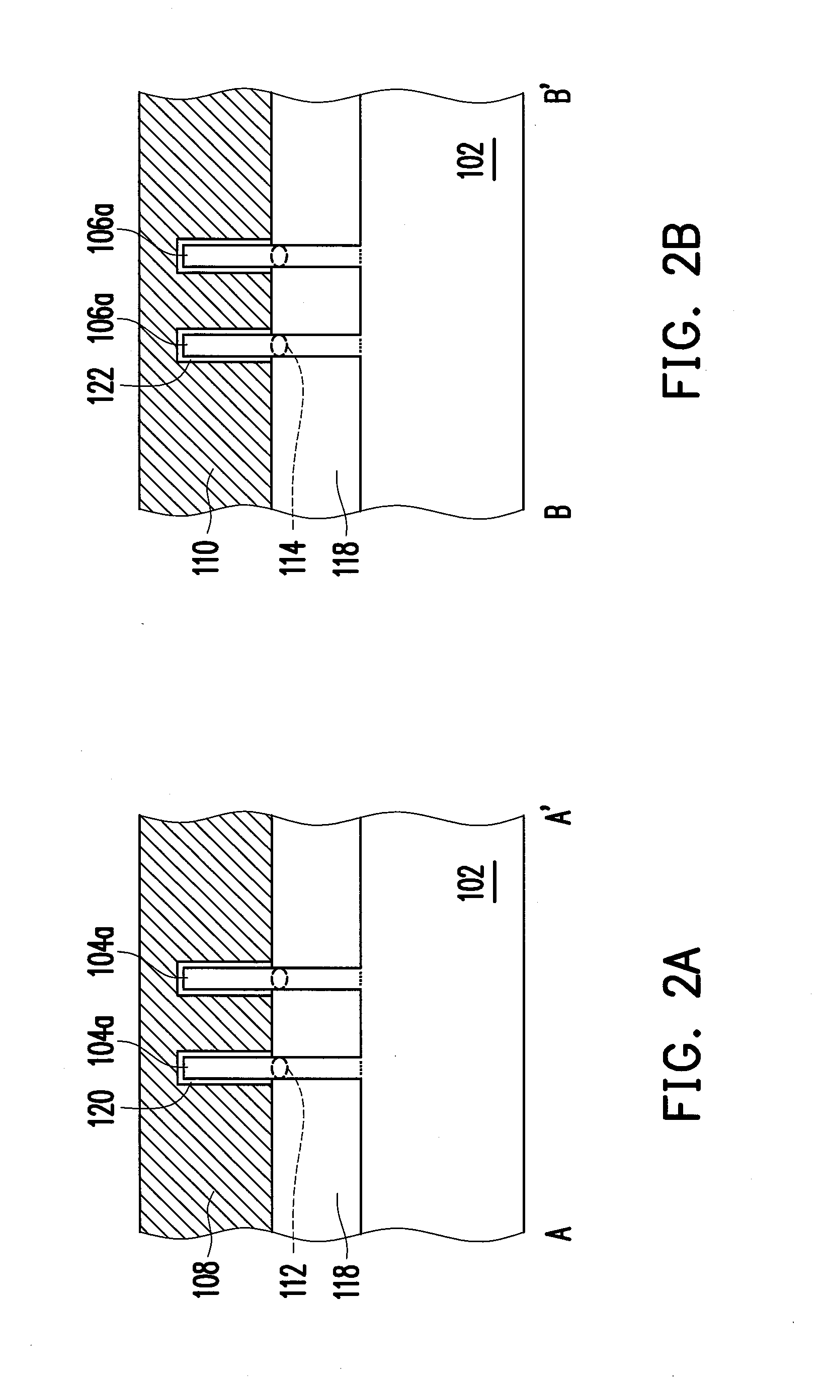
[0026]In a FinFET, one or multiple fins are formed by vertically extending from a substrate, and a gate intersects these fins. A source and a drain are formed at respective ends of each fin, and an effective channel determined by a contact region of each fin and the gate is formed therebetween. As compared with a planar transistor, the FinFET has an increased channel width, and thus, a higher drive current can be obtained with a less chip area in an integrated circuit.

[0027]As devices are continuously miniaturized and compactly integrated, demand for reducing the line width of the fins is raised, so that conventional PESD technique applied at the drain side for lowering breakdown voltage and discharg...


PUM


Abstract

A semiconductor device and a fabricating method thereof are provided. The semiconductor device includes a substrate of a first conductivity type, a fin, a gate, source and drain regions of a second conductivity type, and a first doped region of the second conductivity type. A plurality of isolation structures is formed on the substrate. The fin is disposed on the substrate between two adjacent isolation structures. The gate is disposed on the isolation structures and covers a portion of the fin, wherein the portion of the fin covered by the gate is of the first conductivity type. The source and drain regions is configured in the fin at respective sides of the gate. The first doped region is configured in the fin underlying the source and drain regions and adjoining the substrate. The first doped region has an impurity concentration lower than that of the source and drain regions.

Description

BACKGROUND OF THE INVENTION[0001]1. Field of the Invention[0002]The present invention relates to a semiconductor device and a method for fabricating the same, and more particularly, to an electrostatic discharge (ESD) protection device and a method for fabricating the same that are compatible with a fin-type field effect transistor (FinFET) process.[0003]2. Description of Related Art[0004]ESD is the main factor of electrical overstress (EOS) which causes damage to most of electronic devices or systems. Such damage can result in the permanent damage of semiconductor devices and computer systems, so that circuit functions of integrated circuits (ICs) are affected and operation of electronic products is abnormal. Accordingly, a number of methods have been developed to protect the semiconductor IC devices against possible ESD damages. The most common type of ESD protection is the incorporation of a specific hardware inside the IC package, and therefore a specially-designed ESD protectio...

Claims


Application Information

Patent Timeline
Patent Type & Authority Applications(United States)
IPC IPC(8): H01L27/12H01L21/336
CPCH01L21/823821H01L29/66795H01L21/26513H01L27/0924
Inventor WANG, CHANG-TZUCHAO, MEI-LINGLIN, CHIEN-TING
Owner MARLIN SEMICON LTD
Why Eureka
Try Eureka