Apparatus and Method for Achieving Glitch-Free Clock Domain Crossing Signals

a clock domain and signal technology, applied in the field of digital circuit design, can solve the problems of insufficient functional simulation verification techniques for identifying analog problems, increasing the level of functional and structural complexity of current system-on-a-chip (soc) designs, and increasing the complexity of current system-on-a-chip designs

Active Publication Date: 2013-05-23
ARM FINANCE OVERSEAS LTD
View PDF4 Cites 22 Cited by
  • Summary
  • Abstract
  • Description
  • Claims
  • Application Information

AI Technical Summary

Problems solved by technology

Current System-on-a-chip (SoC) designs contain increased levels of functional and structural complexities within a single system.
Verification of these Clock Domain Crossing (CDC) designs presents daunting challenges since there are issues related to transistor level analog effects.
Traditional Register Transfer Level (RTL) functional simulation verification techniques are insufficient to identify these analog issues.
Known CDC related issues include metastability issues caused by setup and hold-time violations of flip-flops, jitter due to unpredictable delays across clock domains, functional issues due to convergence and divergences of crossover paths and functional issues due to divergence of metastable signals.
Although static timing analysis (STA) is useful, it requires manual inspection, it assumes false paths, and it is prone to errors.
If a gate-level simulation finds a timing violation for any path of a CDC signal, one cannot be sure whether there are any other potential violations in various CDC paths.
Fixing the design at these late stages is also very risky.

Method used


Image

  • Apparatus and Method for Achieving Glitch-Free Clock Domain Crossing Signals
  • Apparatus and Method for Achieving Glitch-Free Clock Domain Crossing Signals
  • Apparatus and Method for Achieving Glitch-Free Clock Domain Crossing Signals

Examples


Embodiment Construction

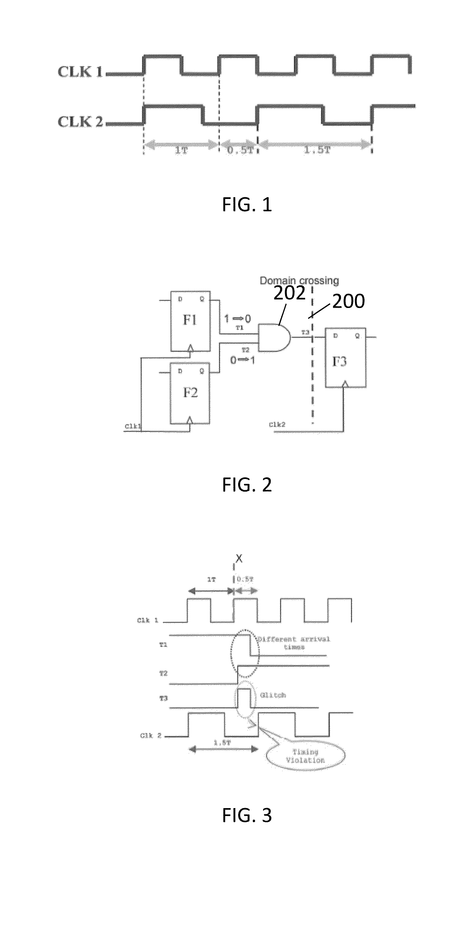
[0019]Consider two synchronous clock domains that can run at various integer and non-integer clock ratios, such as 1:1, 2:1, 3:2, etc. It is important to avoid fractional cycle-times across clock domains. In other words, a timing constraint between flip-flops across clock domains should be at least one cycle-time of the fastest clock.

[0020]FIG. 1 illustrates 3:2 clock ratio waveforms. Signal CLK1 has three cycles for every two cycles of CLK2. The figure illustrates the possible time periods between positive edge to positive edge of faster clock (CLK1) to slower clock (CLK2) at 1 T, 0.5 T and 1.5 T, where T is the cycle time of the faster clock. A design goal is to have a set-up time of at least 1 T cycle time.

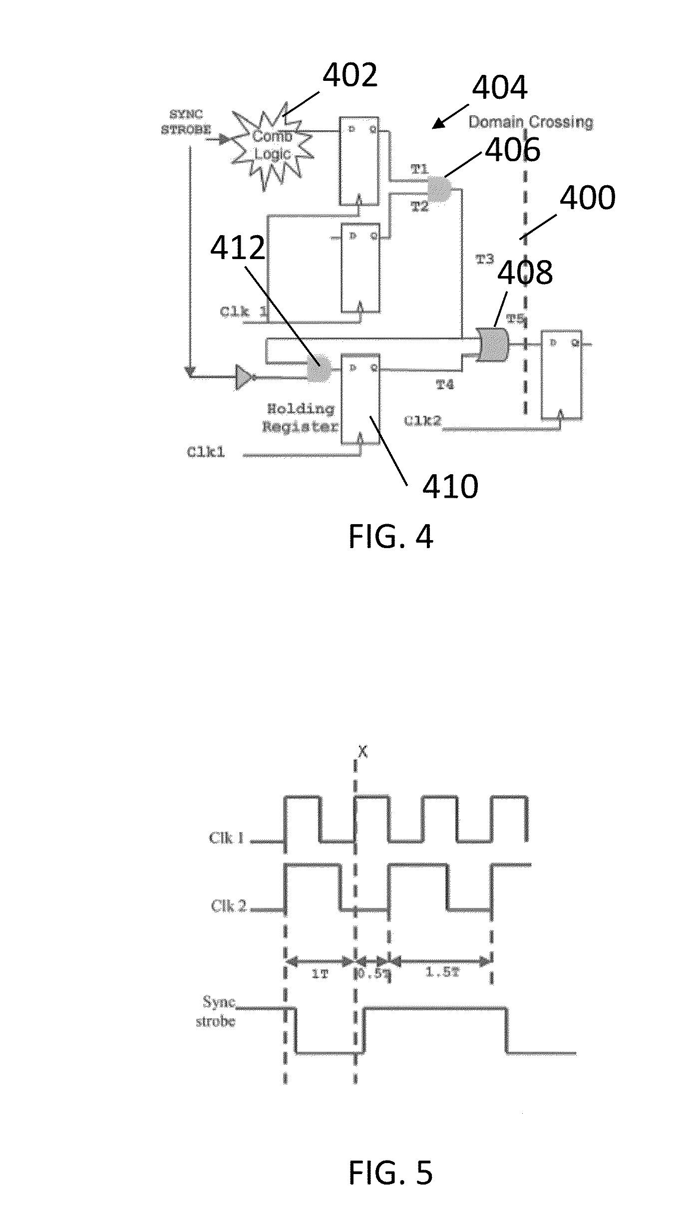
[0021]FIG. 2 illustrates flip-flops F1 and F2 responsive to CLK1. Therefore, the flip-flops are in a faster clock domain. Flip-flop F3 is responsive to CLK2 and therefore is in a slower clock domain. A clock domain crossing is shown with line 200.

[0022]Signals T1 and T2 are lau...


PUM


Abstract

A computer implemented method includes identifying in an original circuit output signals that drive domain crossing logic separating a first clock domain from a second clock domain. A revised circuit is formed with a register attached to the domain crossing logic. The register receives an output signal and a synchronization signal that precludes the output signal from transitioning at selected clock cycle intervals.

Description

CROSS-REFERENCE TO RELATED APPLICATION[0001]This application claims priority to U.S. Provisional Patent Application Ser. No. 61 / 562,975, filed Nov. 22, 2011, entitled, “Achieving Glitch-Free Clock Domain Crossing Signals Using Formal Verification, Static timing Analysis and Sequential Equivalence Checking”, the contents of which are incorporated herein by reference.FIELD OF THE INVENTION[0002]This invention relates generally to digital circuit design. More particularly, this invention relates to techniques for achieving glitch-free clock domain crossing signals.BACKGROUND OF THE INVENTION[0003]Current System-on-a-chip (SoC) designs contain increased levels of functional and structural complexities within a single system. With this integration of multiple design functionalities, various clock domains are introduced for different portions of the SoC. Verification of these Clock Domain Crossing (CDC) designs presents daunting challenges since there are issues related to transistor leve...

Claims


Application Information

Patent Timeline
Patent Type & Authority Applications(United States)
IPC IPC(8): G06F1/12
CPCG06F1/12G06F1/08
Inventor TALUPURU, KESAVA REDDYATHI, SANJAI B.
Owner ARM FINANCE OVERSEAS LTD
Why Eureka
Try Eureka