Method of Manufacturing Sealed Body and Method of Manufacturing Light-Emitting Device
a technology of sealing body and light-emitting device, which is applied in the direction of solid-state devices, electric lighting sources, electric light sources, etc., can solve the problems of reducing the yield of sealed bodies, achieve low reflectivity, reduce the amount of reflected laser light entering the frit glass, and improve the effect of sealing
- Summary
- Abstract
- Description
- Claims
- Application Information
AI Technical Summary
Benefits of technology
Problems solved by technology
Method used
Image
Examples
embodiment 1
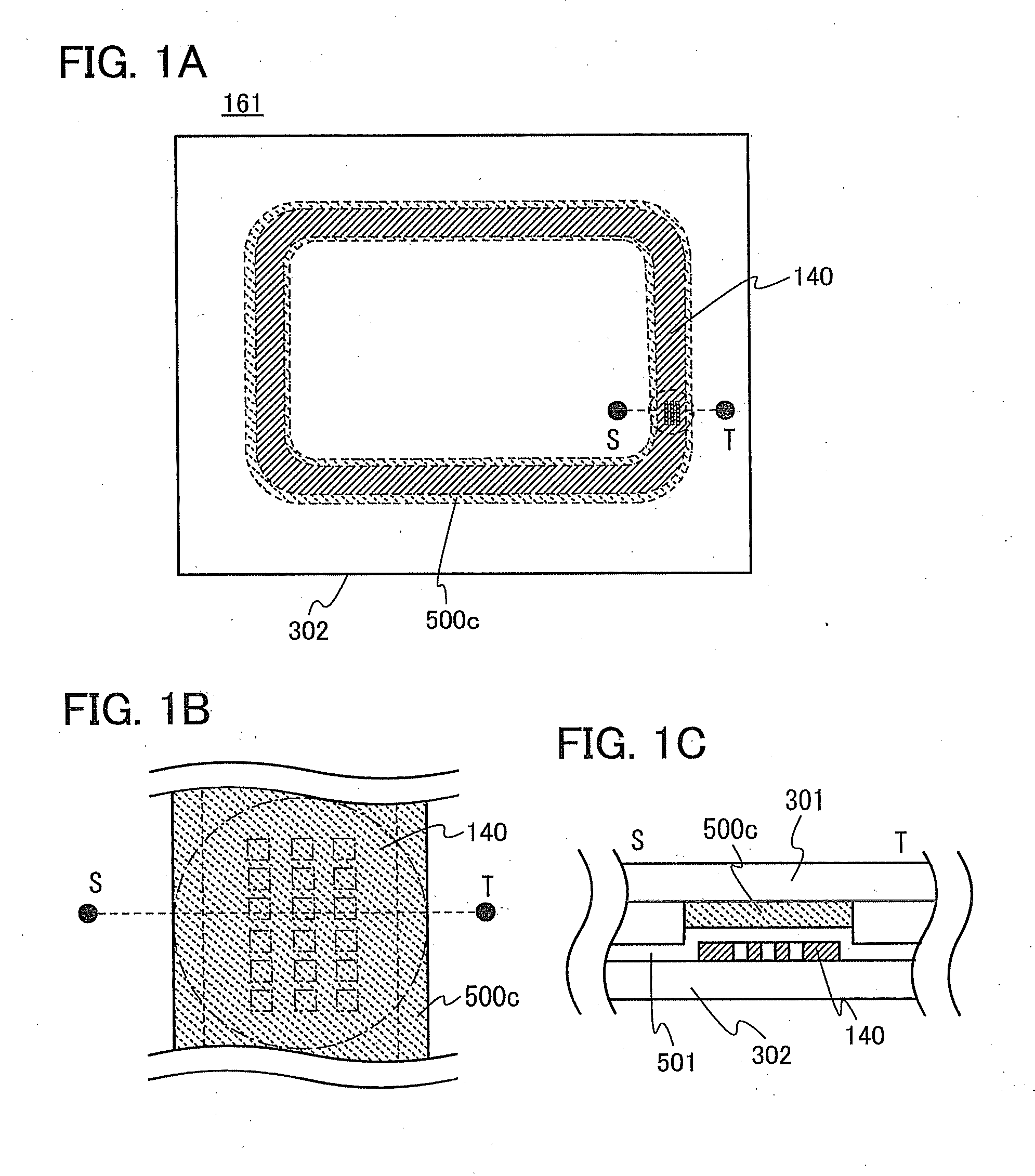
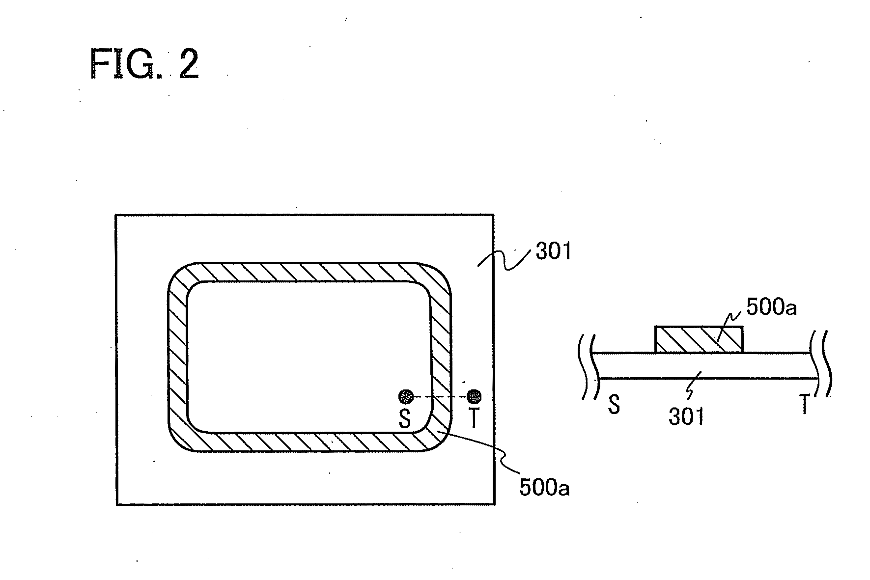
[0038]In this embodiment, a method of manufacturing a sealed body according to one embodiment of the present invention will be described. A method of manufacturing a sealed body 161 in FIGS. 1A to 1C will be described with reference to FIG. 2, FIGS. 3A to 3D, FIGS. 4A to 4D, FIGS. 5A to 5D, and FIGS. 6A to 6C.
(Structure of Sealed Body)
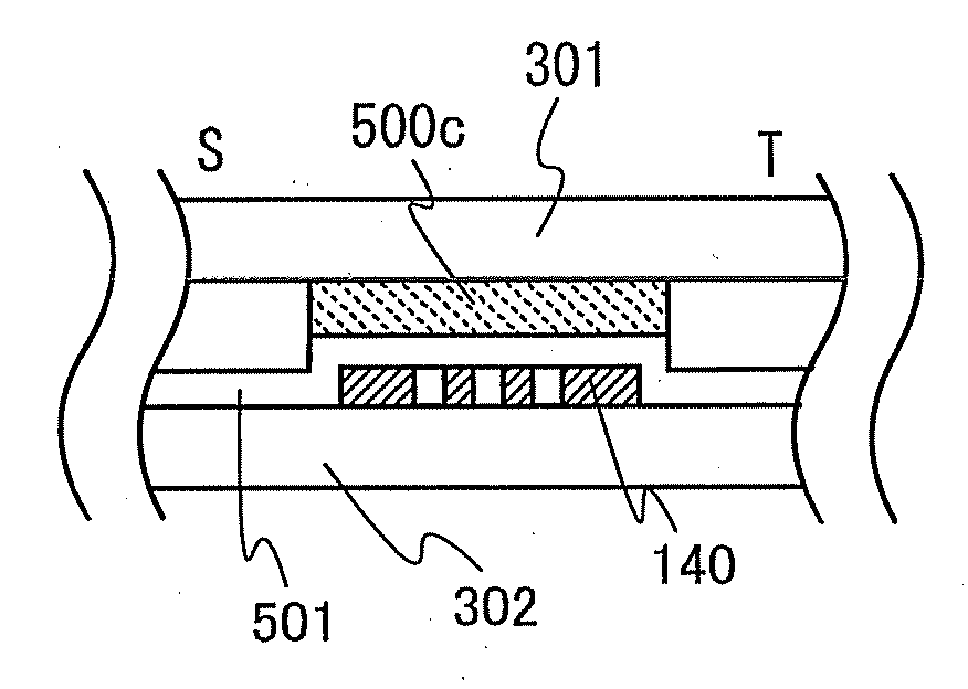
[0039]The sealed body 161 includes a first substrate 301, a second substrate 302, a frit glass layer 500c, a reflective layer 140, and an inorganic insulating layer 501. FIG. 1A is a top view of the sealed body 161. FIG. 1B is a top view in which part of the reflective layer 140 is enlarged, and FIG. 1C is a cross-sectional view taken along dotted line S-T in FIG. 1B. Note that double wave lines in FIGS. 1B and 1C show that some components are not illustrated here.
[0040]In this specification, a frit glass which has been applied as a frit glass paste to a substrate is defined as a frit glass layer 500a, a frit glass obtained by baking the frit glass lay...
embodiment 2
[0065]In this embodiment, a method of manufacturing a light-emitting device according to one embodiment of the present invention will be described. A method of manufacturing a light-emitting device 163 in FIGS. 7A to 7C will be described with reference to FIGS. 8A to 8C and FIGS. 9A to 9C.
(Structure of Light-Emitting Device)
[0066]The light-emitting device 163 includes the first substrate 301, the second substrate 302, the fit glass layer 500c, the reflective layer 140, the inorganic insulating layer 501, an organic EL element 125, a terminal 126a, and a terminal 126b. FIG. 7A is a top view of the light-emitting device 163. FIG. 7B is a top view in which part of the reflective layer 140 is enlarged, and FIG. 7C is a cross-sectional view taken along dotted line S-T in FIG. 7B. Note that double wave lines in FIGS. 7B and 7C show that some components are not illustrated here.
[0067]In this specification, a frit glass which has been applied as a frit glass paste to a substrate is defined ...
embodiment 3
[0092]In this embodiment, one mode of an organic EL element that can be used in a light-emitting device according to one embodiment of the present invention will be described with reference to FIG. 10A.
[0093]In this embodiment, an organic EL element 100 includes a first electrode 101, a light-transmitting conductive layer 103, an organic EL layer 200, and a second electrode 102. The light-transmitting conductive layer 103 is in contact with the first electrode 101. Note that in this embodiment, the following description will be made on the assumption that the first electrode 101 and the light-transmitting conductive layer 103 function as an anode and the second electrode 102 functions as a cathode. In other words, the following description will be made on the assumption that light emission can be obtained when voltage is applied between the first electrode 101 and the second electrode 102 such that the potential of the first electrode 101 is higher than that of the second electrode ...
PUM
| Property | Measurement | Unit |
|---|---|---|
| wavelength | aaaaa | aaaaa |
| thickness | aaaaa | aaaaa |
| thickness | aaaaa | aaaaa |
Abstract
Description
Claims
Application Information


