

Circuit, method and system for overload protection
- Summary
- Abstract
- Description
- Claims
- Application Information
AI Technical Summary
Benefits of technology
Problems solved by technology
Method used
Image

Examples
Embodiment Construction
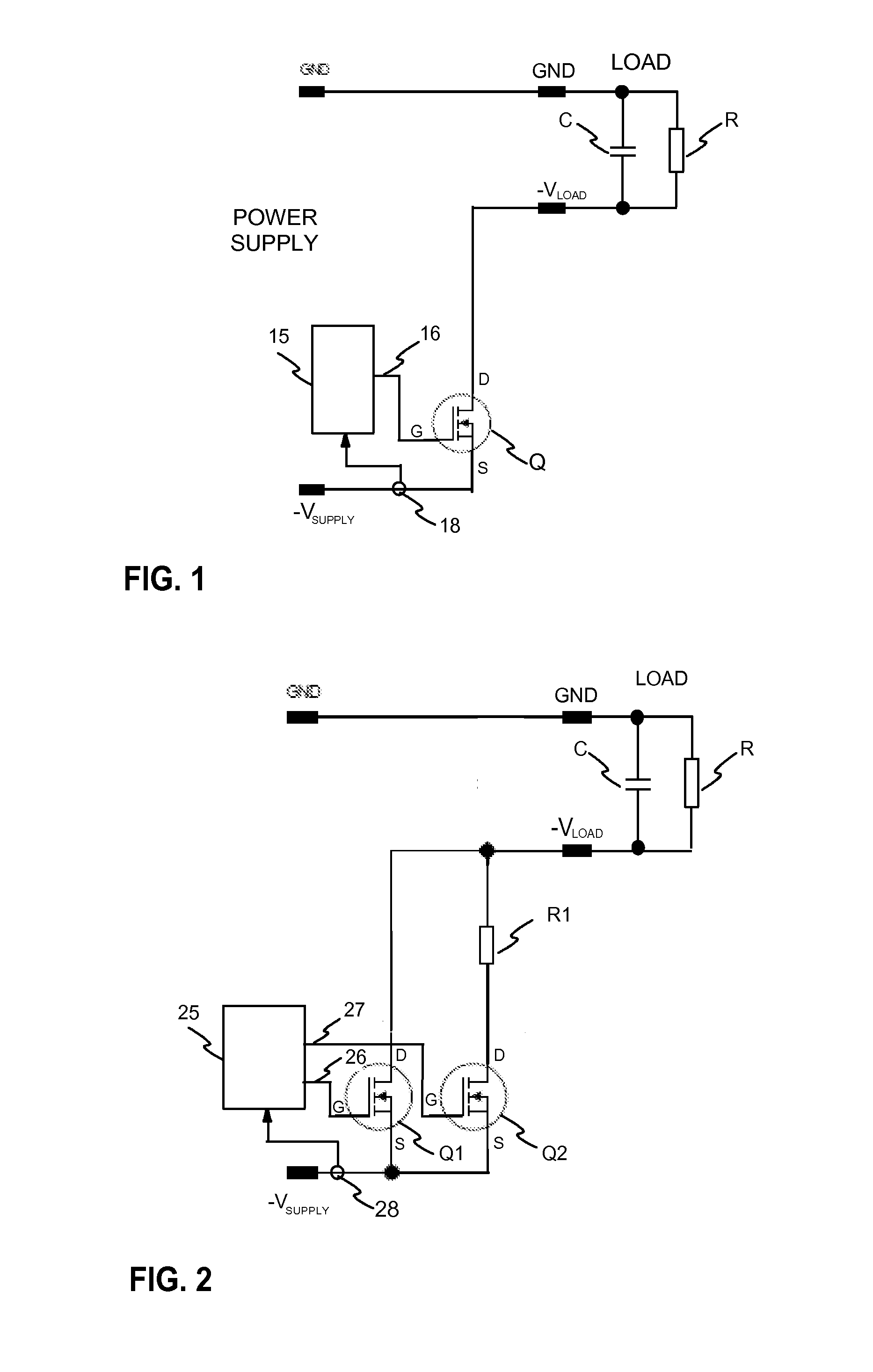
[0048]FIGS. 1 and 2 where described on the prior art part of the description.
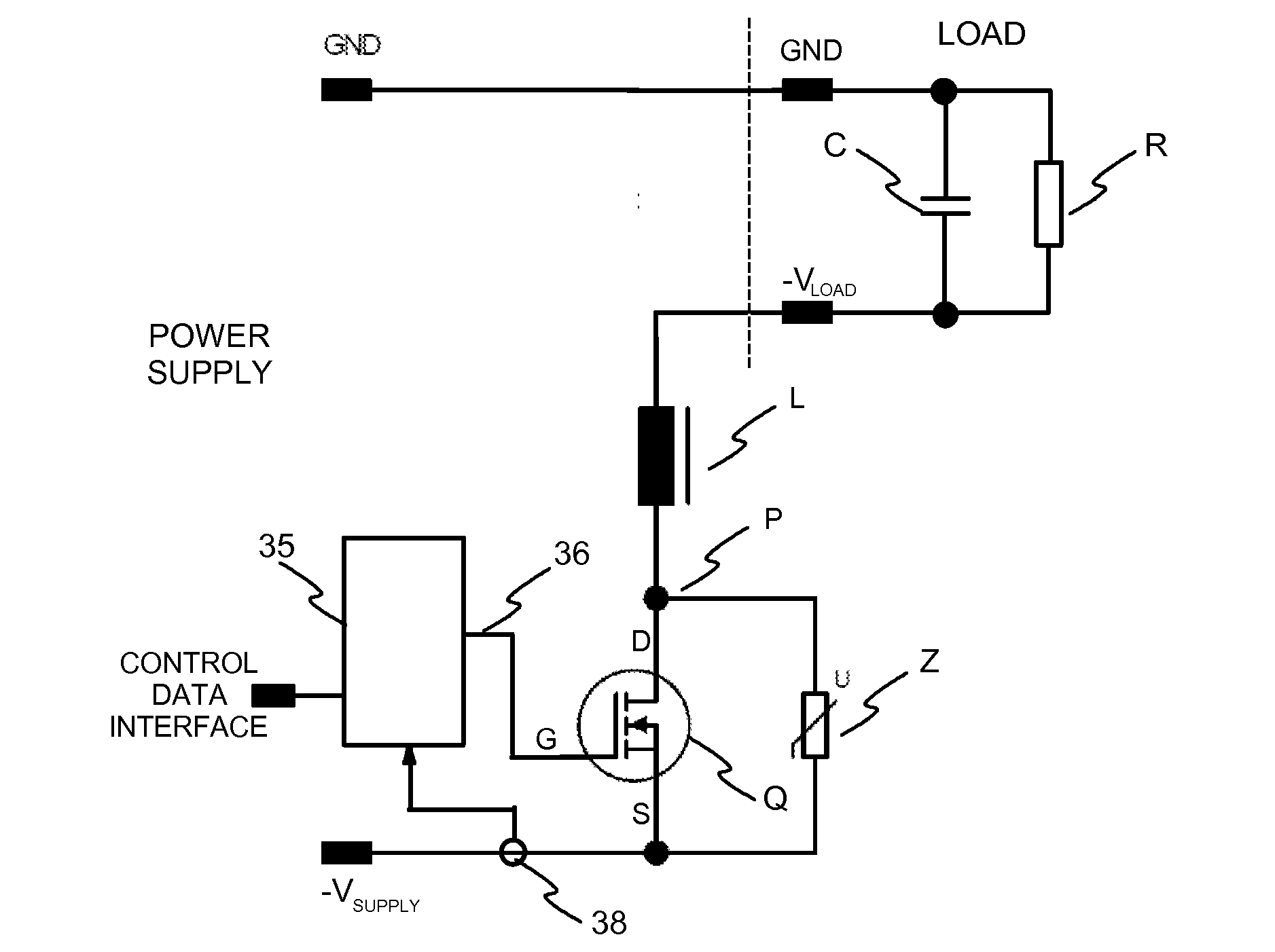
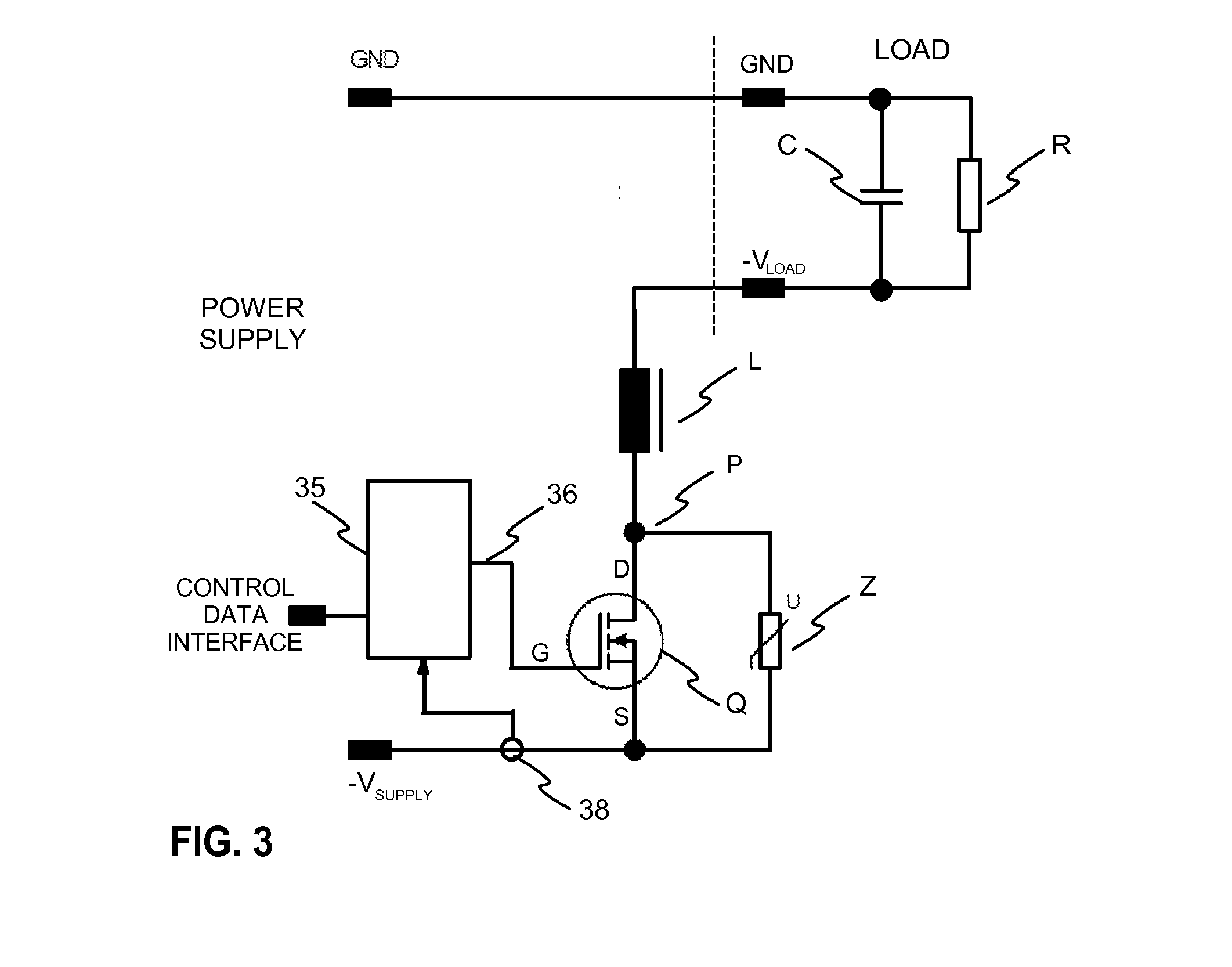
[0049]FIG. 3 illustrates an exemplary overload protection circuit according to the invention. A power supply provides an output voltage between ground GND and negative voltage output −VSUPPLY terminals. The power supply provides power to a load which has terminals for ground GND and negative voltage input −VLOAD. R is used in the Figure to denote resistive load and C is used to denote capacitive load.
[0050]The overload protection circuit has a switching element Q, which may be a power semiconductor, such as MOSFET or an IGBT, for example. The switching transistor is controlled with control means 35, which has a control output 36 connected to the gate G of the switching transistor. The overload protection circuit has an inductor L connected in series with the switching element Q. In the circuit of FIG. 3 the source S of the switching element is connected to the negative terminal −VSUPPLY of the power supply,...
PUM
 Abstract
Description
Claims
Application Information