Semiconductor having integrally-formed enhanced thermal management

a technology of enhanced thermal management and semiconductor devices, which is applied in the direction of semiconductor devices, semiconductor/solid-state device details, electrical devices, etc., can solve the problems of new challenges in heat management and extraction on these devices, unsatisfactory approaches, and many times more expensive than before, and achieve enhanced thermal management of semiconductor devices. , the effect of high heat storage capacity

Inactive Publication Date: 2013-06-13
ADVANCED COOLING TECH
View PDF2 Cites 154 Cited by
  • Summary
  • Abstract
  • Description
  • Claims
  • Application Information

AI Technical Summary

Benefits of technology

[0015]A thermal management material having a relatively high thermal capacitance is filled in the containment gap. This thermal management material enhances the thermal management of the semiconductor device by thermally coupling the localized heat generation area to the material in the containment gap which has a high heat storage capacity. This allows the semiconductor to safely release more heat when operating under pulsed conditions while remaining below the maximum allowable junction temperature of the device.

Problems solved by technology

The extremely high power densities available in nitride devices create new challenges for heat management and extraction on these devices.
However, this approach is not ideal.
SiC substrates are typically only available on 4″ diameters, are many times more expensive than Si, and are still severely limit by heat dissipation.
In addition, in spite of the unprecedented power densities demonstrated in these devices, commercial GaN devices typically operate at much lower power densities (4-6 W / mm) due to the great difficulty in dissipating the generated waste heat.
Even when operating at the relatively low power densities of 4 W / mm, for proper operation these devices need to be attached to large heat sinks, appreciably limiting the system scalability and effective packaging.
During pulsed device operation, the GaN material at the chip level rapidly rises in temperature, as its low mass is not able to absorb the generated heat.
However, use of this material and others is often costly and impedes chip manufacturability because these materials are expensive and difficult to work with.

Method used


Image

  • Semiconductor having integrally-formed enhanced thermal management
  • Semiconductor having integrally-formed enhanced thermal management
  • Semiconductor having integrally-formed enhanced thermal management

Examples


Embodiment Construction

[0031]For purposes of promoting an understanding of the principles of the invention, reference will now be made to the embodiments illustrated in the drawings and specific language will be used to describe the same. It will nevertheless be understood that no limitation of the scope of the invention is thereby intended, there being contemplated such alterations and modifications of the illustrated device, and such further applications of the principles of the invention as disclosed herein, as would normally occur to one skilled in the art to which the invention pertains.

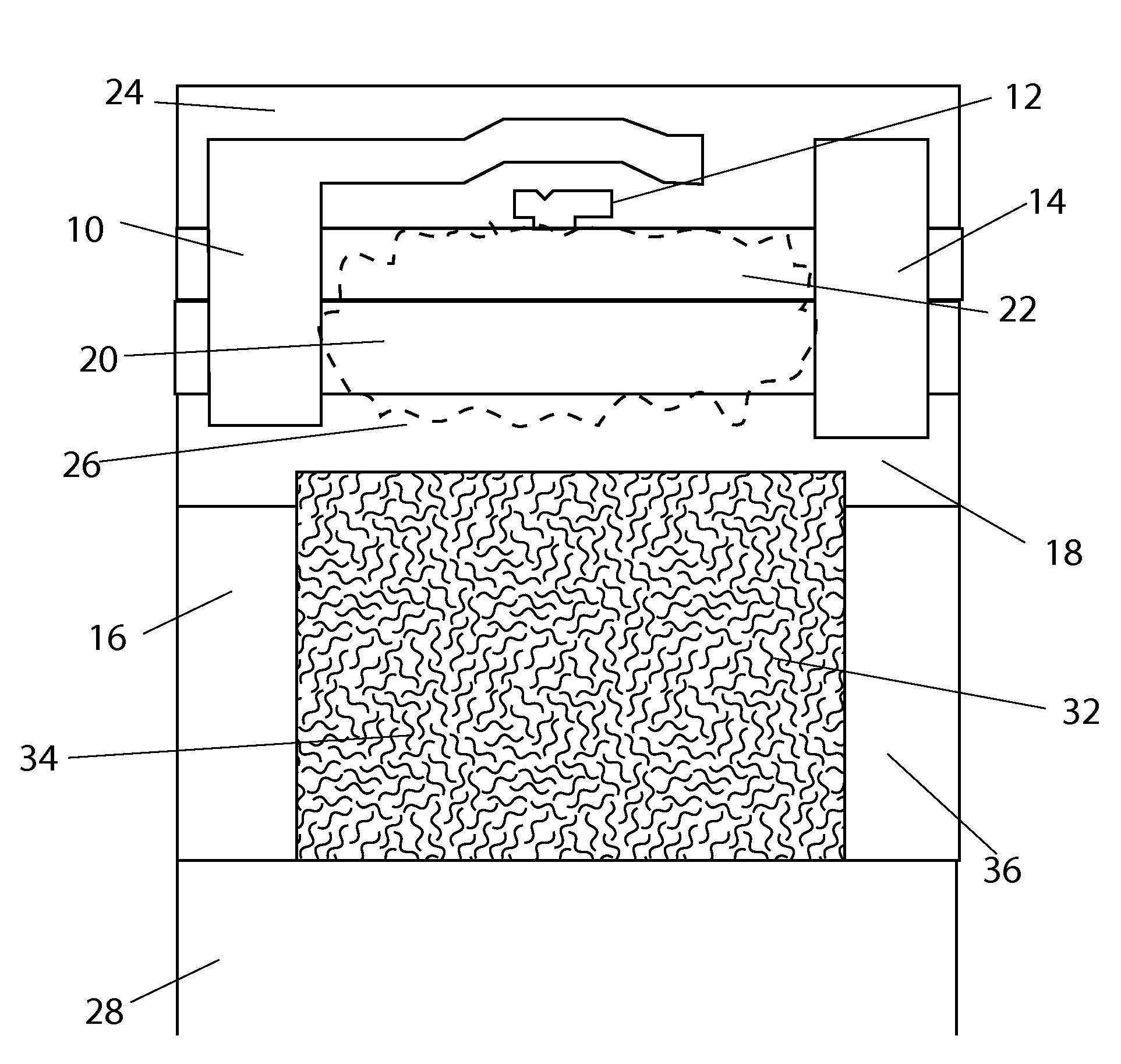
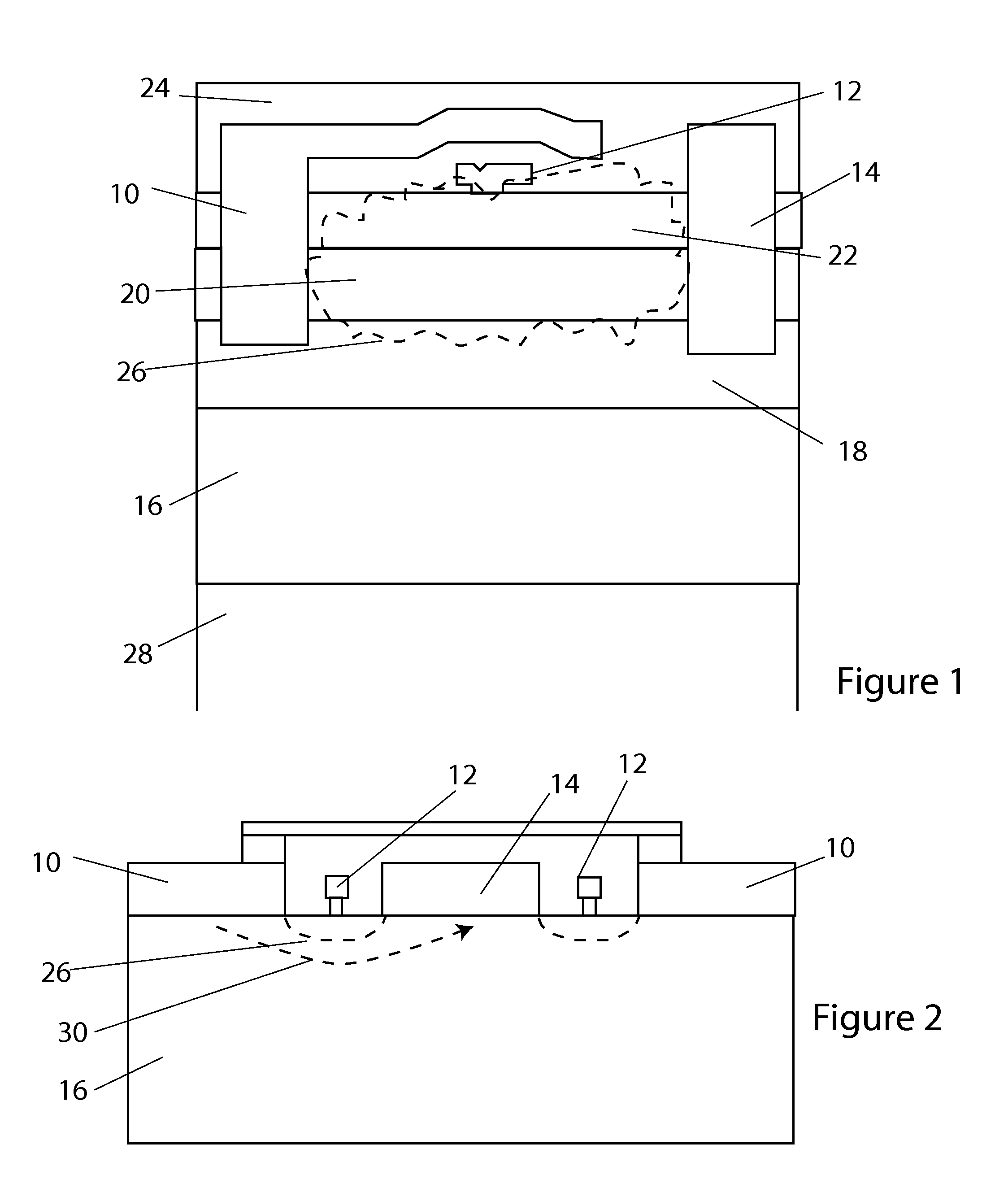
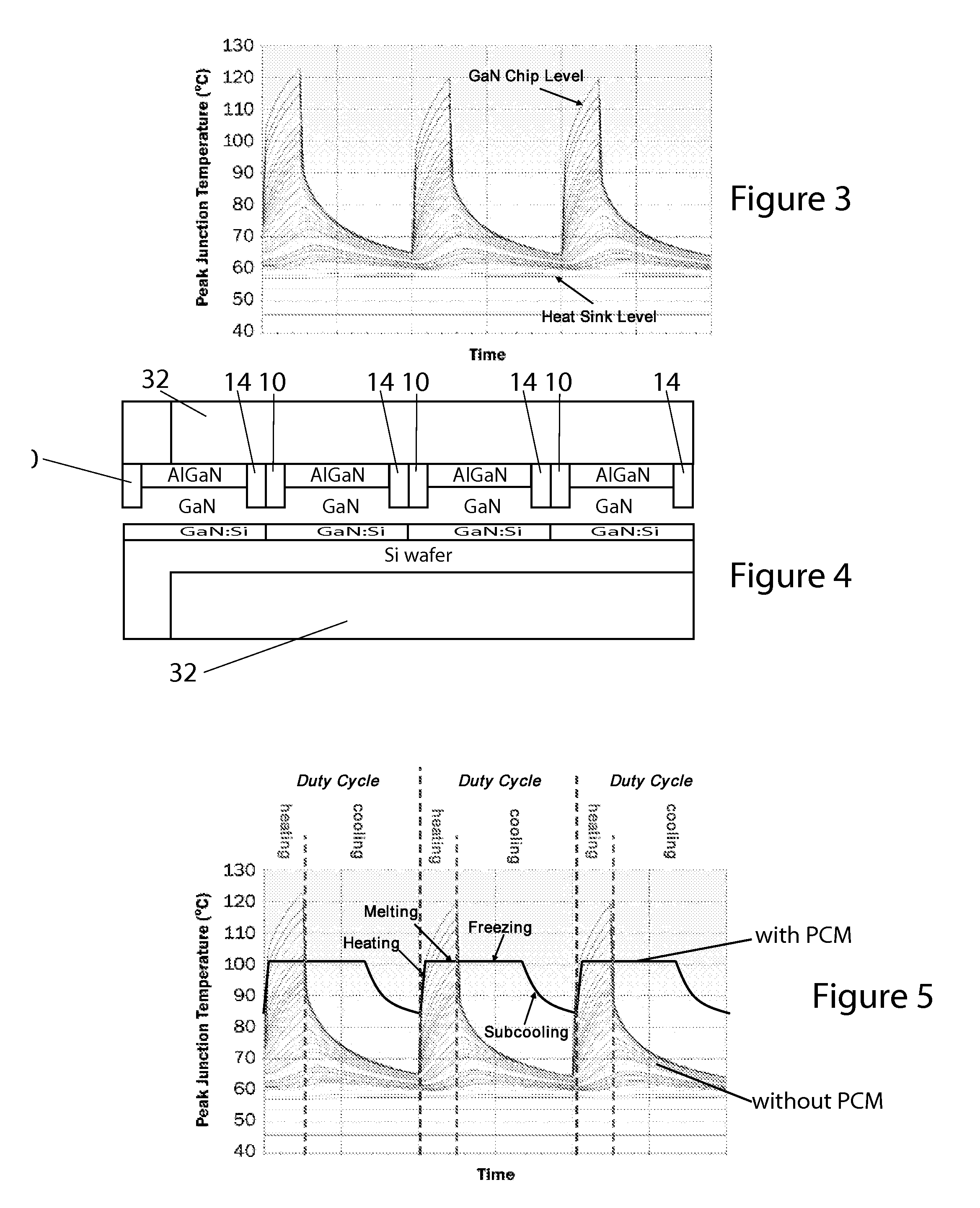
[0032]In accordance with the present invention, a phase change material (PCM) is disposed immediately adjacent to the source of heat in an operating semiconductor device, such as the location between the source and drain of a GaN transistor. The PCM is utilized to reduce the junction temperature and stabilize the operating temperatures in pulsed GaN devices by absorbing the rapid temperature transients observed in GaN...


PUM


Abstract

A semiconductor structure and method of manufacturing that has integrally-formed enhanced thermal management. During operation of a semiconductor device, electron flow between the source and the drain creates localized heat generation. A containment gap is formed by selectively removing a portion of the back side of the semiconductor device substrate directly adjacent to a localized heat generation area. A thermal management material is filled in the containment gap. This thermal management material enhances the thermal management of the semiconductor device by thermally coupling the localized heat generation area to a heat sink. The thermal management material may be a Phase Change Material (PCM) having a heat of fusion effective for absorbing heat generated in the localized heat generation area by the operation of the semiconductor device for reducing a peak operating temperature of the semiconductor device.

Description

BACKGROUND OF THE INVENTION[0001]The present invention pertains to a semiconductor device having integrally-formed enhanced thermal management. Specifically, the present invention pertains to a semiconductor device, such as a gallium nitride transistor (GaN), that can be effectively formed on a substrate, such as silicon (Si), having integrally-formed enhanced thermal management so that transistors can be packed at higher device densities and operated at significantly higher power densities under pulsed operating conditions.[0002]Recently, AlGaN / GaN high electron mobility transistors (HEMTs) have become a preferred option for solid-state amplifiers in the 1-40 GHz frequency range. With an output power density of more than 40 W / mm at 4 GHz, these devices offer an order of magnitude higher power density than Si-based electronics, higher efficiency levels, lower cooling requirements and easier impedance matching (U. K. Mishra, L. Shen, T. E. Kazior, and Y.-F. Wu, “GaN-based RF power de...

Claims


Application Information

Patent Timeline
Patent Type & Authority Applications(United States)
IPC IPC(8): H01L23/488H01L21/50
CPCH01L29/402H01L29/41766H01L29/7786H01L29/2003H01L2924/0002H01L23/367H01L2924/00
Inventor BONNER, III, RICHARD WILLIAMDESAI, TAPAN
Owner ADVANCED COOLING TECH
Why Eureka
Try Eureka