Phosphor film, method of manufacturing the same, coating method of phosphor layer, method of manufacturing LED package, and LED package manufactured thereby

a technology of phosphor film and phosphor particles, which is applied in the manufacture of electrode systems, natural mineral layered products, and the manufacture of electric discharge tubes/lamps. it can solve the problems of difficult application to a case in which a phosphor is coated with respect to individual chips, light scattering may increase, and the dispersion of phosphor particles may be deteriorated in the resin, etc., to achieve uniform thickness, reduce the effect of modules and easy coating

Inactive Publication Date: 2013-06-13
SAMSUNG ELECTRONICS CO LTD
View PDF2 Cites 33 Cited by
  • Summary
  • Abstract
  • Description
  • Claims
  • Application Information

AI Technical Summary

Benefits of technology

[0043]As set forth above, in a phosphor film according to an embodiment of the present invention, a phosphor layer may be configured to have properties in which it is in a partially cured state and a modulus is reduced upon being heated, such that the phosphor layer can be coated to have a uniform thickness around a light emitting chip. In particular, even in a case in which a wire-bonded light emitting chip is coated, the coating of a phosphor layer may be obtained without transformation of a wire.
[0044]In a method of manufacturing a phosphor film, a method of coating a light emitting diode (LED) chip with a phosphor layer, a method of manufacturing an LED package, and an LED package manufactured thereby: a phosphor film may be manufactured to have a form in which the phosphor layer can be easily coated on the LED chip; and a phosphor layer may be coated to have a uniform thickness around various types of LED chips by using the same, whereby a light emitting device having excellent quality of light may be manufactured.

Problems solved by technology

Thus, various conformal LED chip coating techniques have been proposed, but since a majority of the techniques are applied prior to a wire bonding process, the application thereof are limited to a flip-chip type package or an additional process is required to open a separate wire bonding pad part during phosphor coating.
Further, such a technique is used in a free mold lead frame-type packaging process and may be difficult to be applied to a case in which a phosphor is coated with respect to individual chips.
Here, a solid phase of inorganic phosphor particles have partial sedimentation during a coating process, even after being dispensed, until a phosphor paste is cured, due to a relatively low viscosity being required for implementation of the coating process, within a tube storing matters in equipment, and therefore, dispersibility of phosphor particles may be deteriorated in a resin, and light scattering may be increased.

Method used


Image

  • Phosphor film, method of manufacturing the same, coating method of phosphor layer, method of manufacturing LED package, and LED package manufactured thereby
  • Phosphor film, method of manufacturing the same, coating method of phosphor layer, method of manufacturing LED package, and LED package manufactured thereby
  • Phosphor film, method of manufacturing the same, coating method of phosphor layer, method of manufacturing LED package, and LED package manufactured thereby

Examples


Embodiment Construction

[0067]Hereinafter, embodiments of the present invention will be described in detail with reference to the accompanying drawings. The invention may, however, be embodied in many different forms and should not be construed as being limited to the embodiments set forth herein. Rather, these embodiments are provided so that this disclosure will be thorough and complete, and will fully convey the scope of the invention to those skilled in the art.

[0068]In the drawings, the shapes and dimensions of elements may be exaggerated for clarity, and the same reference numerals will be used throughout to designate the same or like elements.

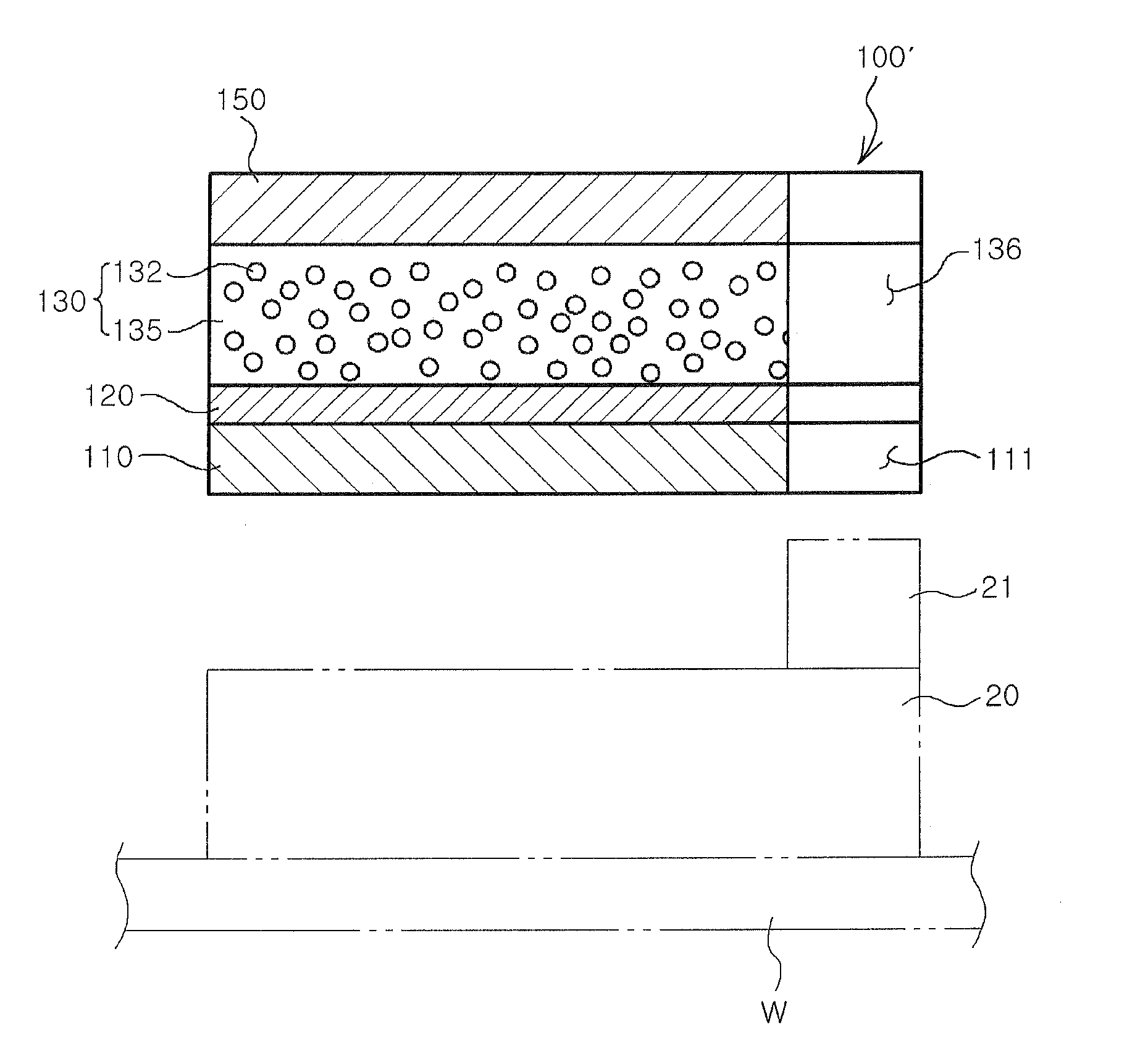
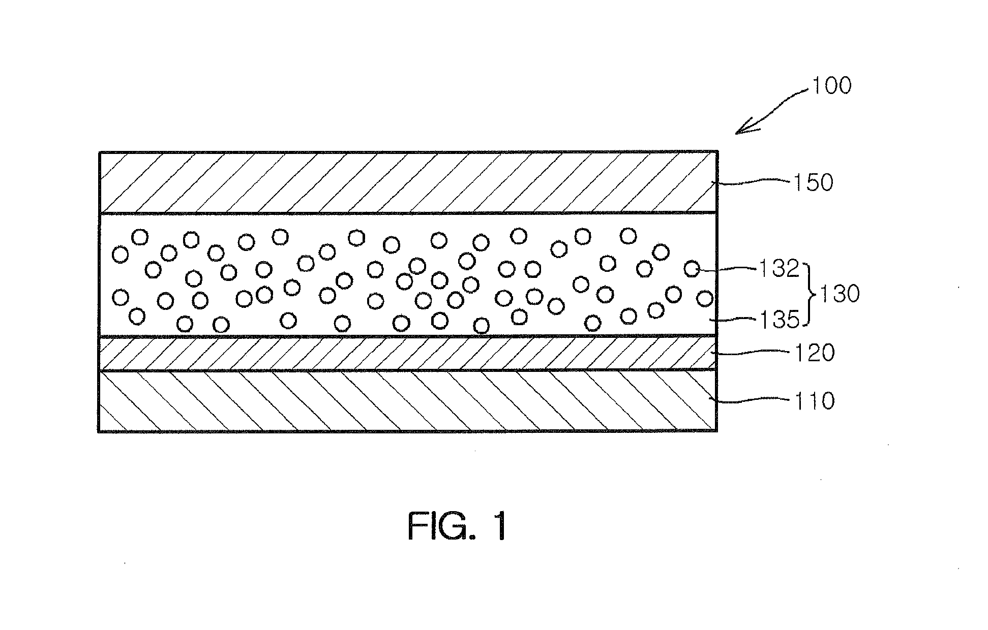
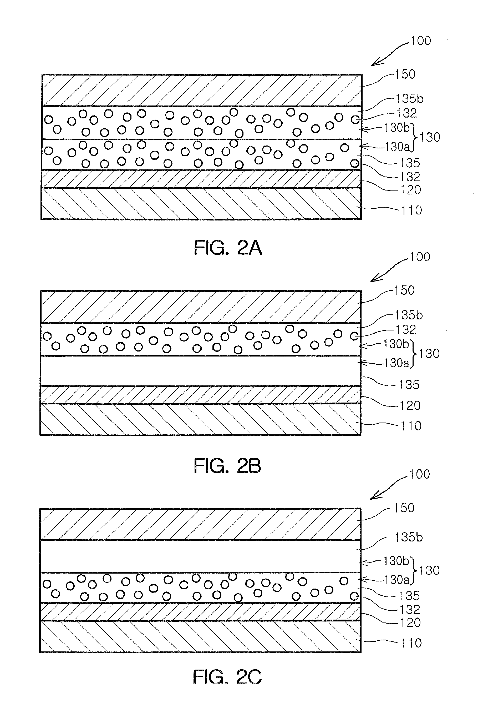
[0069]FIG. 1 illustrates a structure of a phosphor film according to an embodiment of the present invention. FIGS. 2A through 2C schematically illustrate a structure of a phosphor layer in the phosphor film of FIG. 1. FIGS. 3 and 4 illustrate a structure according to variation examples of the phosphor film of FIG. 1.

[0070]With reference to FIGS. 1 to 4, a phosp...


PUM

PropertyMeasurementUnit
temperatureaaaaaaaaaa

Abstract

There are provided a phosphor film, a method of manufacturing the same, and a method of coating an LED chip with a phosphor layer. The phosphor film includes: a base film; a phosphor layer formed on the base film and obtained by mixing phosphor particles in a partially cured resin material; and a cover film formed on the phosphor layer to protect the phosphor layer.

Description

TECHNICAL FIELD [0001]The present invention relates to a phosphor film, a method of manufacturing the same, a coating method of coating a light emitting diode (LED) chip with a phosphor layer, a method of manufacturing a light emitting device package, and a light emitting device package manufactured thereby.BACKGROUND ART [0002]A light emitting diode (LED), known as a next generation light source, has many positive attributes such as a relatively long lifespan, low power consumption, a rapid response rate, environmentally friendly characteristics, and the like, as compared with a light source according to the related art, and has been used as an important light source in various products such as illumination devices and back light units for display devices. In particular, Group III nitride-based LEDs including GaN, AlGaN, InGaN, InAlGaN, and the like have been used in semiconductor light emitting devices outputting blue or ultraviolet light.[0003]In general, a reflective layer is fo...

Claims


Application Information

Patent Timeline
Patent Type & Authority Applications(United States)
IPC IPC(8): H01L33/50
CPCC09K11/06Y10T428/24802B32B27/00H01L2933/0041B32B19/00H01L33/505B05D5/06H01L2224/48091Y10T428/24942B32B3/10Y10T428/24893B32B5/16Y10T428/24851H01L33/50H01L2924/00014H05B33/22B32B3/08B32B3/14B32B3/16B32B3/18B32B7/12B32B9/04B32B9/045B32B27/06B32B27/08B32B27/32B32B2250/03B32B2250/40B32B2250/44B32B2266/025B32B2307/40B32B2307/422B32B2457/00H01L2224/45139H01L2924/00011H01L24/97H01L2224/48227H01L2224/8592H01L2924/181Y10T428/31855H01L2924/00H01L2924/00012H01L2924/01049H01L2924/01005
Inventor KWAK, CHANG HOONPARK, IL WOOLEE, KYU JINYOO, CHEOL JUNHONG, SEONG JAE
Owner SAMSUNG ELECTRONICS CO LTD
Why Eureka
Try Eureka