Eureka AIR delivers breakthrough ideas for toughest innovation challenges, trusted by R&D personnel around the world.

Laminated sheet and method of manufacturing semiconductor device using the laminated sheet

Inactive Publication Date: 2013-06-13
NITTO DENKO CORP
View PDF6 Cites 2 Cited by
  • Summary
  • Abstract
  • Description
  • Claims
  • Application Information

AI Technical Summary

Benefits of technology

The present invention provides a laminated sheet that can prevent resin composition layer adhesion and electrical reliability issues. Additionally, it allows for easy peeling of a back grinding tape from multiple semiconductor elements after dicing. A method of manufacturing a semiconductor device using this laminated sheet is also provided.

Problems solved by technology

However, greater man-hours are required because the synthetic resin film that is also diced into individual pieces cannot be peeled from a plurality of the semiconductor chips collectively and has to be peeled individually.
Because of that, water is absorbed by the adhesive composition for a semiconductor during dicing, and it causes a generation of space and voids in a layer of the adhesive composition for a semiconductor during flip-chip mounting.
Because of these, a decrease in adhering strength and a deterioration in electrical reliability may occur.

Method used


Image

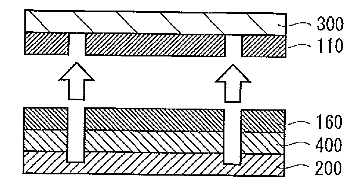
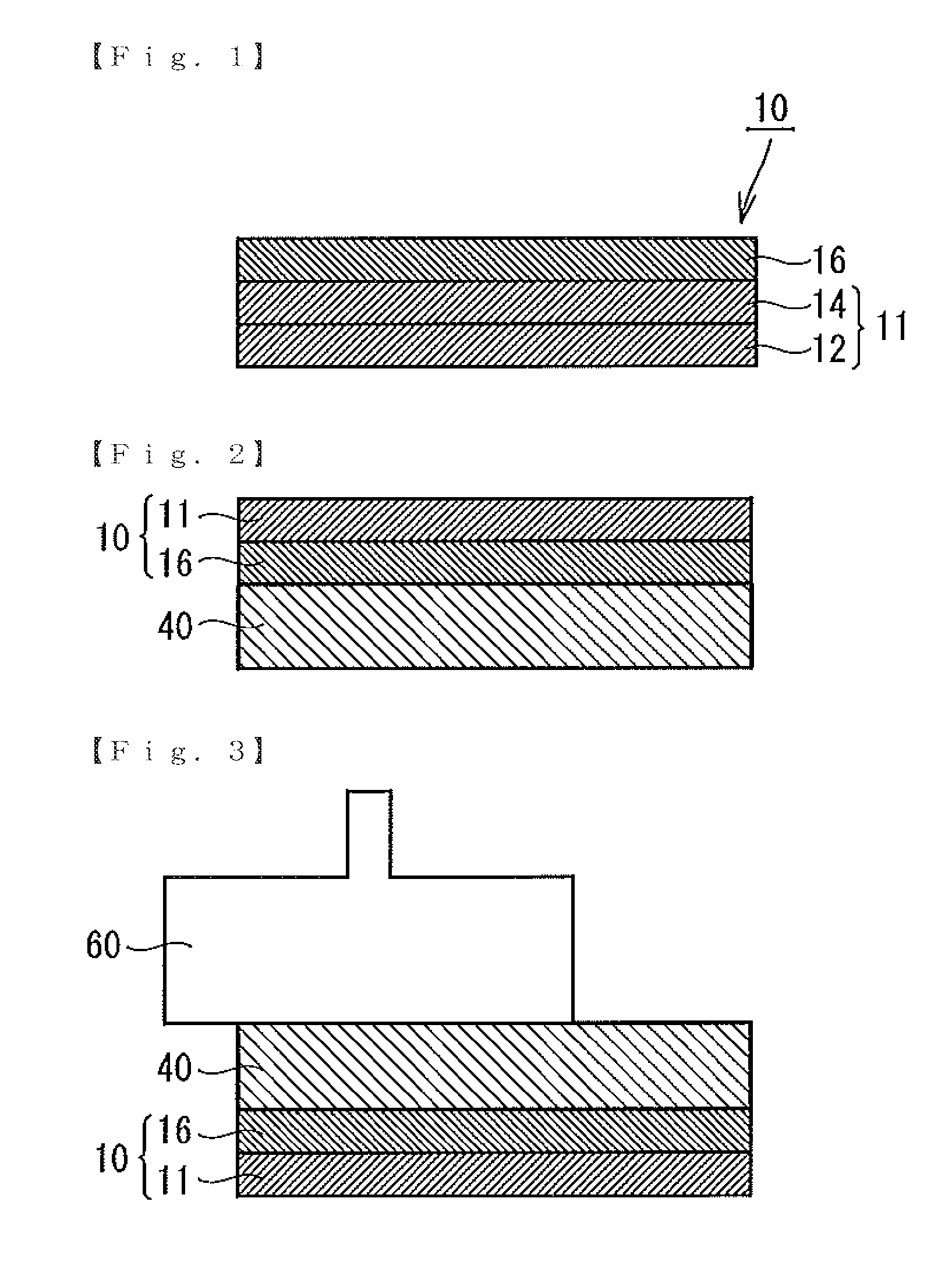
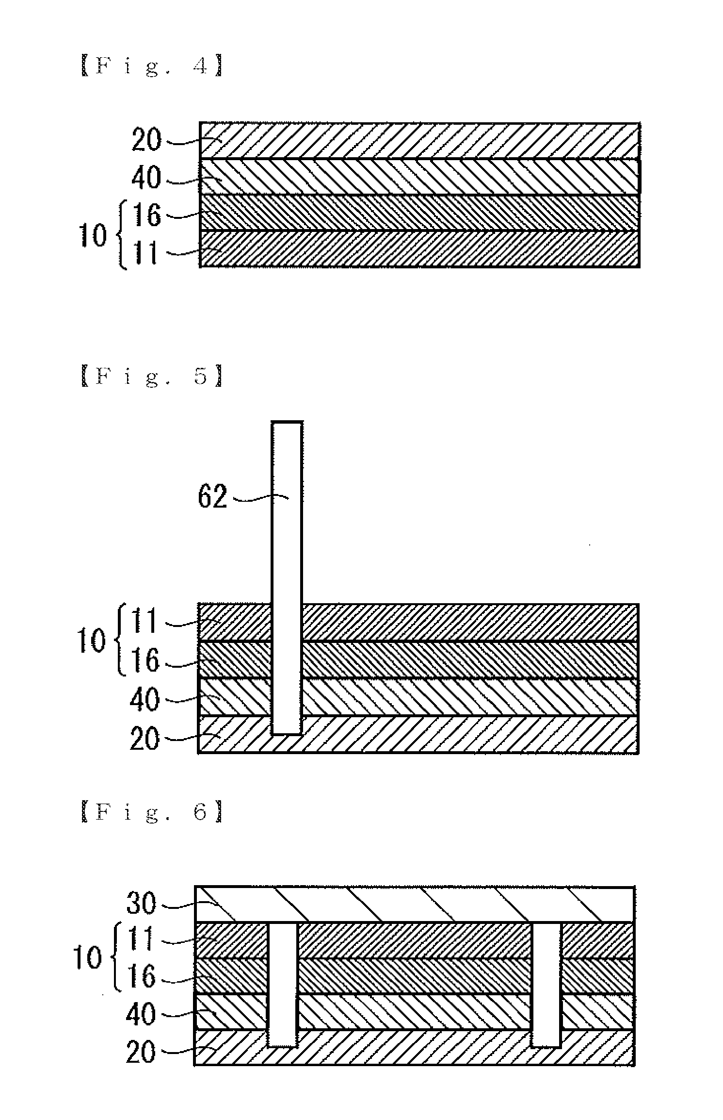
  • Laminated sheet and method of manufacturing semiconductor device using the laminated sheet
  • Laminated sheet and method of manufacturing semiconductor device using the laminated sheet
  • Laminated sheet and method of manufacturing semiconductor device using the laminated sheet

Examples


example 1

[0199]One hundred parts of 2-ethylhexylacrylate and 20 parts of 2-hydroxyethylacrylate were charged in a reactor equipped with a cooling tube, a nitrogen gas introducing tube, a thermometer, and a stirrer. A polymerization process was performed in a toluene solution in a nitrogen gas flow at 60° C. for 8 hours to obtain an acrylic polymer A.

[0200]Fifteen parts of 2-methacryloyloxyethylisocyanate was added to the acrylic polymer A, and subjected to an addition polymerization reaction process in an air flow at 50° C. for 12 hours to obtain an acrylic polymer A′.

[0201]Then, 2 parts of a polyisocyanate crosslinking agent (product name “Coronate L”, manufactured by Nippon Polyurethane Industry Co., Ltd.) and 2 parts of an acetophenone photopolymerization initiator (product name “Irgacure 651”, manufactured by Chiba Specialty Chemicals Corporation) were added to 100 parts of the acrylic polymer A′ to obtain a pressure-sensitive adhesive composition solution A.

[0202]The pressure-sensitive ...

example 2

[0203]The same back grinding tape as the back grinding tape A of Example 1 was defined as a back grinding tape B according to Example 2. The pressure-sensitive adhesive layer that configures the back grinding tape B was defined as a pressure-sensitive adhesive layer B. The back grinding tape B according to Example 2 was irradiated with an ultraviolet ray of 50 mJ / cm2 after dicing and before pasting of the pressure-sensitive adhesive tape as described later, and used.

example 3

[0204]The same back grinding tape as the back grinding tape A of Example 1 was defined as a back grinding tape C according to Example 3. The pressure-sensitive adhesive layer that configures the back grinding tape C was defined as a pressure-sensitive adhesive layer C. The back grinding tape C according to Example 3 was irradiated with an ultraviolet ray of 400 mJ / cm2 after pasting of the pressure-sensitive adhesive tape as described later, and used.


PUM

PropertyMeasurementUnit
Temperatureaaaaaaaaaa
Pressureaaaaaaaaaa
Energyaaaaaaaaaa

Abstract

The present invention provides a laminated sheet that can prevent the decrease in adhering strength of a resin composition layer and the deterioration in electrical reliability and in which a back grinding tape can be peeled from a plurality of semiconductor elements collectively after dicing. The laminated sheet has a back grinding tape in which a pressure-sensitive adhesive layer is formed on a base, and a resin composition layer that is provided on the pressure-sensitive adhesive layer of the back grinding tape, wherein the tensile modulus of the pressure-sensitive adhesive layer at 23° C. is 0.1 to 5.0 MPa, and the T-peeling strength between the pressure-sensitive adhesive layer and the resin composition layer is 0.1 to 5 N / 20 mm at 23° C. and 300 mm / min.

Description

BACKGROUND OF THE INVENTION[0001]1. Field of the Invention[0002]The present invention relates to a laminated sheet and a method of manufacturing a semiconductor device using the laminated sheet.[0003]2. Description of the Related Art[0004]In recent years, thinning and downsizing of a semiconductor device and its packaging have been further required. Because of that, a flip-chip semiconductor device, in which a semiconductor element such as a semiconductor chip is mounted on a substrate by flip-chip bonding, has been widely used for semiconductor devices and their packaging. In flip-chip bonding, a circuit surface of a semiconductor chip is fixed to an electrode forming surface of the substrate in such a way that the circuit surface is facing the electrode forming surface.[0005]After flip-chip bonding, a space is formed between the semiconductor element and the substrate, and the space has been conventionally filled with a sealing material such as a sealing resin. However, there is a...

Claims


Application Information

Patent Timeline
IPC IPC(8): B32B3/30H01L21/78C09J7/20C09J7/38
CPCB32B3/30H01L21/78B23B3/30H01L24/27H01L24/29H01L24/81H01L24/83H01L2224/13111H01L2224/13144H01L2224/13147H01L2224/27436H01L2224/29023H01L2224/2919H01L2224/73104H01L2224/73204H01L2224/81191H01L2224/81203H01L2224/83191H01L2224/83203H01L2224/83855H01L2224/9211H01L2224/94H01L2224/16227H01L2224/16245H01L2224/32225H01L2224/32245C09J7/02C09J2201/36C09J2201/606C09J2201/61C09J2201/622C09J2203/326C09J2463/00H01L2221/68327H01L2221/6834H01L2221/68377H01L2221/68381H01L2221/68386H01L21/6836Y10T428/24355H01L2224/27H01L2224/8385H01L2924/00014H01L2924/01082H01L2924/0103H01L2924/01083H01L2924/01047H01L2924/01029H01L2924/00H01L2924/15787H01L2224/16225C09J7/20C09J7/38Y10T428/31511C09J2301/208C09J2301/304C09J2301/302C09J2301/312H01L23/29H01L23/28
Inventor SENZAI, HIROYUKITANAKA, SHUMPEIMIZUNO, KOJI
Owner NITTO DENKO CORP
Why Eureka
Eureka Blog
Learn More