Conformal metallization process for the fabrication of semiconductor laser devices

a semiconductor laser and metallization process technology, applied in semiconductor lasers, laser details, electrical devices, etc., can solve the problems of au migration into the inp material, affect the uniformity of the deposited layer, etc., and reduce the possibility of au migration

Inactive Publication Date: 2013-06-27
EMCORE INC
View PDF4 Cites 1 Cited by
  • Summary
  • Abstract
  • Description
  • Claims
  • Application Information

AI Technical Summary

Benefits of technology

[0011]In an embodiment, the metal contact portion is formed by depositing, in a single deposition process: a layer of titanium so as to contact the semiconductor substrate through the contact opening; then a layer of platinum; then a layer of gold; then a layer

Problems solved by technology

Sudden failure is a problem which can afflict semiconductor laser devices.
One cause of such sudden

Method used


Image

  • Conformal metallization process for the fabrication of semiconductor laser devices
  • Conformal metallization process for the fabrication of semiconductor laser devices
  • Conformal metallization process for the fabrication of semiconductor laser devices

Examples


Embodiment Construction

[0023]Details of the present invention will now be described, including exemplary aspects and embodiments thereof. Referring to the drawings and the following description, like reference numbers are used to identify like or functionally similar elements, and are intended to illustrate major features of exemplary embodiments in a highly simplified diagrammatic manner. Moreover, the drawings are not intended to depict every feature of actual embodiments nor the relative dimensions of the depicted elements, and are not drawn to scale.

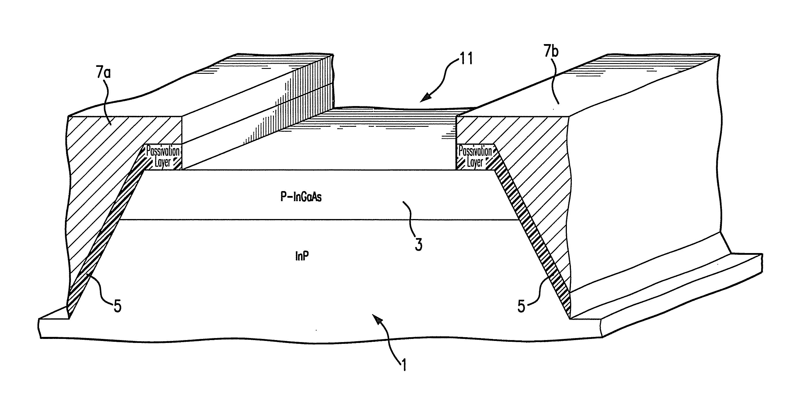
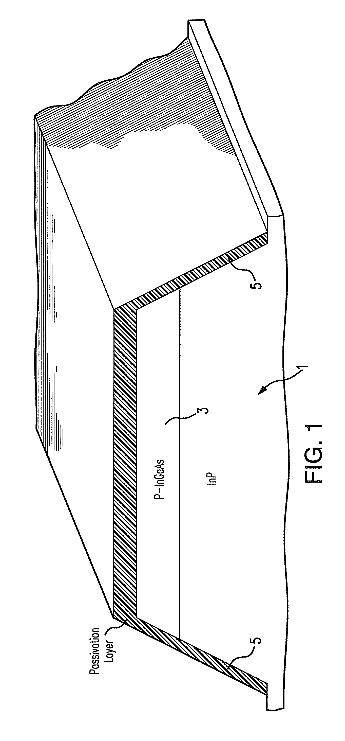
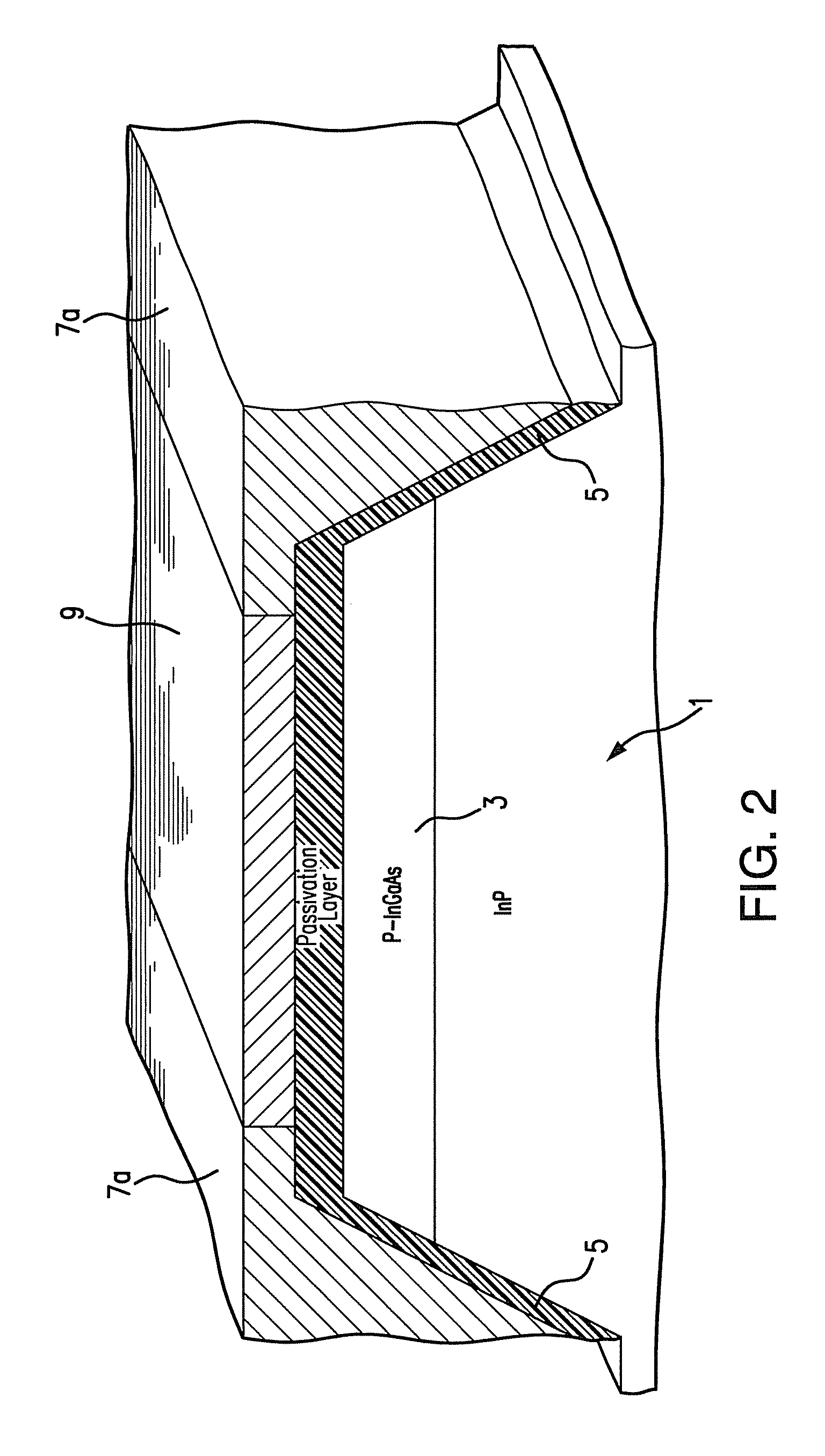
[0024]As shown in FIG. 1, in an embodiment of the present invention a mesa structure 1 forms part of a semiconductor laser device. In this embodiment, the semiconductor laser device is a tunable laser in the frequency region around 1.5 μm fabricated using an Indium Phosphide (InP) semiconductor system. In particular, the semiconductor laser device is formed by the deposition of lattice-matched layers on an InP substrate. FIGS. 1 to 11 schematically illustr...


PUM


Abstract

A method of fabricating a semiconductor laser device by forming a semiconductor structure at least part of which is in the form of a mesa structure having a flat top. The steps include depositing a passivation layer over the mesa structure, forming a contact opening in the passivation layer on the flat top of the mesa structure; and depositing a metal contact portion, with the deposited metal contact portion contacting the semiconductor structure via the contact opening. The contact opening formed through the passivation layer has a smaller area than the flat top of the mesa structure to allow for wider tolerances in alignment accuracy. The metal contact portion comprises a platinum layer between one or more gold layers to provide an effective barrier against Au diffusion into the semiconductor material.

Description

BACKGROUND OF THE INVENTION[0001]1. Field of the Invention[0002]The present invention relates to the fabrication of a semiconductor laser device, and in particular to the formation of a metal contact forming part of the semiconductor laser device.[0003]2. The Background Art[0004]Semiconductor laser devices are widely available. One type of semiconductor laser device is tunable around the 1.5 μm wavelength for use in DWDM optical communications. Such semiconductor laser devices may be based on an InP semiconductor system.[0005]One way of forming a p-metal contact on an InP semiconductor system is to deposit a lattice-matched InGaAs layer, followed by the deposition of layers of Titanium (Ti), Platinum (Pt) and Gold (Au) to form a so-called non-alloyed ohmic contact. The Au layer forms a contact pad, while the Pt layer acts as a barrier to inhibit diffusion of gold into the semiconductor structure. The article “Au / Pt / Ti contacts to p-In0.53Ga0.47As and n-InP layers formed by a single ...

Claims


Application Information

Patent Timeline
IPC IPC(8): H01S5/323H01L21/02
CPCH01S5/0425H01S5/0282H01S5/22H01S2301/176H01S5/04252
Inventor HUANG, JIA-SHENGTHAI, PHONG
Owner EMCORE INC
Why Eureka
Try Eureka