Substrate having transparent conductive layer, method for producing same, transparent conductive film laminate for touch panel, and touch panel

a technology conductive layer, which is applied in the direction of conductive layer on insulating support, instruments, transportation and packaging, etc., can solve the problems of difficult production process, low resistance and high transmittance of transparent conductive film, and easy visualization of differences in haze due to fibrous conductive substance, etc., to achieve easy visual recognition, easy to recognize, and easy to distinguish optical properties

Inactive Publication Date: 2013-07-04
DAINIPPON INK & CHEM INC
View PDF6 Cites 79 Cited by
  • Summary
  • Abstract
  • Description
  • Claims
  • Application Information

AI Technical Summary

Benefits of technology

[0041]A substrate having a transparent conductive layer of the present invention includes a transparent conductive layer pattern on a transparent substrate. Although the substrate includes two regions, i.e., a conductive region and a high-resistance region, the difference in optical properties between the regions is small, so that the transparent conductive pattern is not easily recognized. A method of the present invention for producing a substrate having a transparent conductive layer does not require precise processing at the time of the formation of the transparent conductive pattern. A substrate or film having a transparent conductive layer can be formed only by a method including an application step or a printing step using a coating material for a transparent conductive layer or an ink for a transparent conductive layer, a patterned transparent conductive layer being provided on a transparent substrate or a transparent film substrate, and the transparent conductive layer pattern being not easily visually recogni

Problems solved by technology

In addition, the transparent conductive film advantageously has low resistance and high transmittance.
However, there is a problem in which a difference in haze due to fibrous conductive substance is easily visualized.
In these cases, the production process is complicated.
The registration is difficult.
In the case of using the chloride solution as described in PTL 5, there is a problem of the reaction of silver in the pattern formation region of the transparent conductive film inherently having satisfactory conductivity which should be maintained.
The conductive pattern is not easily visually recognized.
However, it is often difficult to form the isolated pattern region by a usual pattern formation method in such a manner that a visually unrecognizable width between the conductive region and the isolated pattern region is achieved and that both regions are reliably insulated from each other.
In particular, in the case where an applicat

Method used


Image

  • Substrate having transparent conductive layer, method for producing same, transparent conductive film laminate for touch panel, and touch panel
  • Substrate having transparent conductive layer, method for producing same, transparent conductive film laminate for touch panel, and touch panel
  • Substrate having transparent conductive layer, method for producing same, transparent conductive film laminate for touch panel, and touch panel

Examples


example 1

Synthesis of Silver Nanowires

[0236]Silver nanowires are synthesized by a method in which a polyol is used, the method being described in Y. Sun, B. Gates, B. Mayers, & Y. Xia, “Crystalline silver nanowires by soft solution processing” Nano letters, (2002), 2(2) 165-168, then by dissolving silver sulfate in ethylene glycol in the presence of polyvinylpyrrolidone (PVP), and reducing the silver sulfate. Specifically, nanowires used in the present invention were synthesized by the amended polyol method described in U.S. Provisional Patent Application No. 60 / 815,627 applied by Cambrios Technologies Corporation.

[Formation of Transparent Conductive Layer]

[0237]An aqueous dispersion (ClearOhm™, Ink-A AQ, manufactured by Cambrios Technologies Corporation) containing, as metal nanowires to form a transparent conductive layer, 0.5% w / v silver nanowires synthesized by the foregoing method and having a minor axis diameter of about 70 nm to 80 nm and an aspect ratio of 100 or more in an aqueous m...

example 2

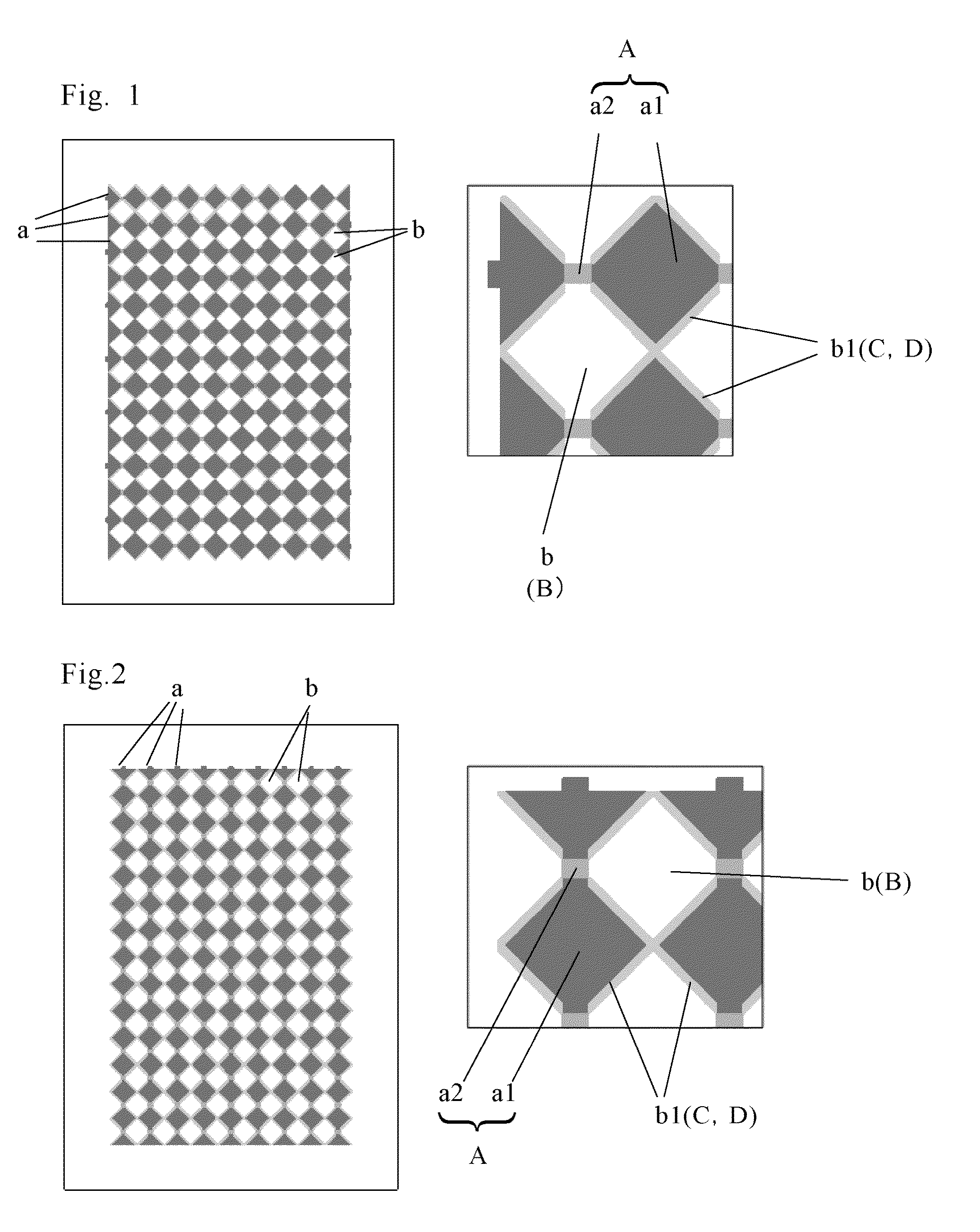
[0249]Unlike Example 1, as a dummy pattern configured to improve viewability, conductive dummy pattern regions, in which dot-like regions not covered with the transparent conductive films and having a diameter of 30 μm were arranged with a pitch of 73 μm, were formed in the linking portions which were formed of the transparent conductive films and which connected the electrode portions to each other. Furthermore, insulating dummy pattern regions, in which dot-like regions covered with the transparent conductive films and having a diameter of 30 μm were arranged with a pitch of 73 μm, were formed in the gap portions where no transparent conductive film is present when the X electrodes were orthogonally superimposed on the Y electrodes.

[0250]The former linking portions that connected the electrode portions to each other were conductive and had conductivity comparable to that of the electrode portions. The haze value of the linking portions was 70% of that of the electrode line portion...


PUM


Abstract

A substrate having a transparent conductive layer has a transparent conductive pattern that is not easily visually recognizable by a naked human eye on a transparent substrate and can be formed by a simple and efficient method. In the case where a transparent conductive pattern is formed on a transparent substrate, the pattern region does not include conductive regions covered with uniform transparent conductive films or a high-resistance region that is not covered with the transparent conductive film, the high-resistance region electrically insulating the conductive regions. Instead of the conductive regions or the high-resistance region, the inventors use a region having a structure including a mixture of a portion covered with the transparent conductive film and a portion not covered with the transparent conductive film, thereby solving the foregoing visual recognition issue.

Description

TECHNICAL FIELD[0001]The present invention relates to a substrate having a transparent conductive layer, the substrate having a transparent conductive layer with a patterned transparent conductive region on a transparent substrate, in which the transparent conductive region and other regions have very similar optical properties, so the transparent conductive region is not optically visualized, and relates to a touch panel produced by bonding the substrates having transparent conductive layers. In particular, the present invention relates to a film having a transparent conductive layer, the film being a transparent film substrate as the foregoing substrate, and to a film having a transparent conductive layer used for the production of a capacitive touch panel. Furthermore, the present invention relates to methods for producing the substrate having a transparent conductive layer and the film having a transparent conductive layer, a transparent conductive film laminate for a touch pane...

Claims


Application Information

Patent Timeline
IPC IPC(8): H05K1/02B05D5/12
CPCY10T428/236G06F2203/04103H05K1/0296B05D5/12G06F3/044G06F2203/04111G06F3/041G06F3/0412G06F3/0445G06F3/0446G06F3/0443H01B5/14
Inventor YAMAZAKI, YOSHIKAZUHAYAKAWA, SATOSHIYOKOKAWA, MIHO
Owner DAINIPPON INK & CHEM INC
Why Eureka
Try Eureka