Silicon carbide semiconductor element and method for fabricating the same

Active Publication Date: 2013-07-04
PANASONIC INTELLECTUAL PROPERTY MANAGEMENT CO LTD
View PDF3 Cites 59 Cited by
  • Summary
  • Abstract
  • Description
  • Claims
  • Application Information

AI Technical Summary

Benefits of technology

[0025]A silicon carbide semiconductor element as an aspect of the present invention has a trench at a (0001) Si plane and the trench has an upper corner region, which is defined by a different surface from the Si plane or a surface that defines the sidewall of the trench, over the sidewall. That is why the gate insulating film can be thicker on the upper corner region than on the upper surface of the silicon carbide layer (i.e., on the Si plane). On top of that, since the end

Problems solved by technology

However, in a MISFET 1000 with such a trench gate structure, the gate insulating film 6 on the inner wall of the tre

Method used


Image

  • Silicon carbide semiconductor element and method for fabricating the same
  • Silicon carbide semiconductor element and method for fabricating the same
  • Silicon carbide semiconductor element and method for fabricating the same

Examples


embodiment 1

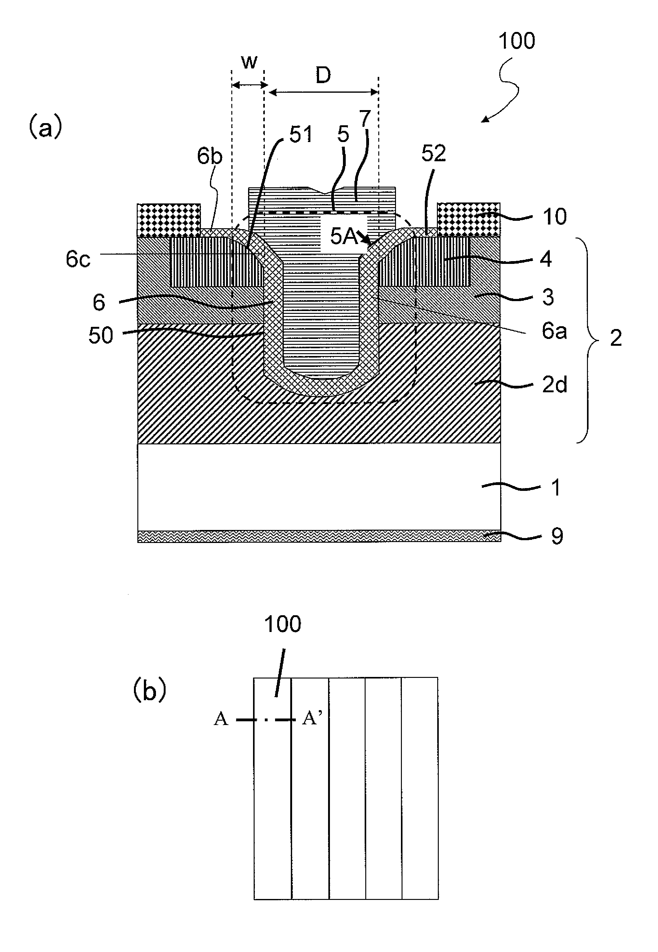
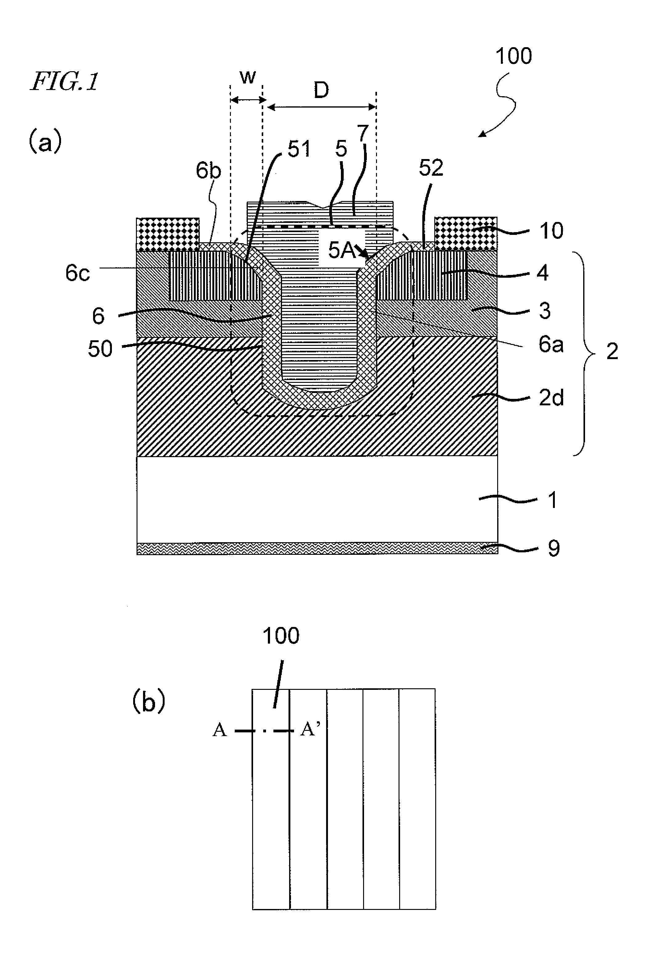
[0056]The structure of a silicon carbide semiconductor element as a first embodiment will be described specifically with reference to FIG. 1. The silicon carbide semiconductor element of this embodiment is a silicon carbide MISFET with a trench gate structure.

[0057]The silicon carbide semiconductor element of this embodiment includes a plurality of unit cells that are arranged two-dimensionally. FIG. 1(a) is a cross-sectional view illustrating one of those unit cells 100 and FIG. 1(b) is a plan view illustrating an exemplary arrangement of the unit cell 100 on the surface of the silicon carbide layer of the semiconductor element. FIG. 1(a) is a cross-sectional view as viewed on the plane A-A′ shown in FIG. 1(b).

[0058]The unit cell 100 includes a silicon carbide substrate 1 with a (0001) Si plane. In this embodiment, the unit cell 100 further includes a silicon carbide layer (such as an epitaxial layer) 2 which is arranged on the (principal) surface of the silicon carbide substrate 1...

embodiment 2

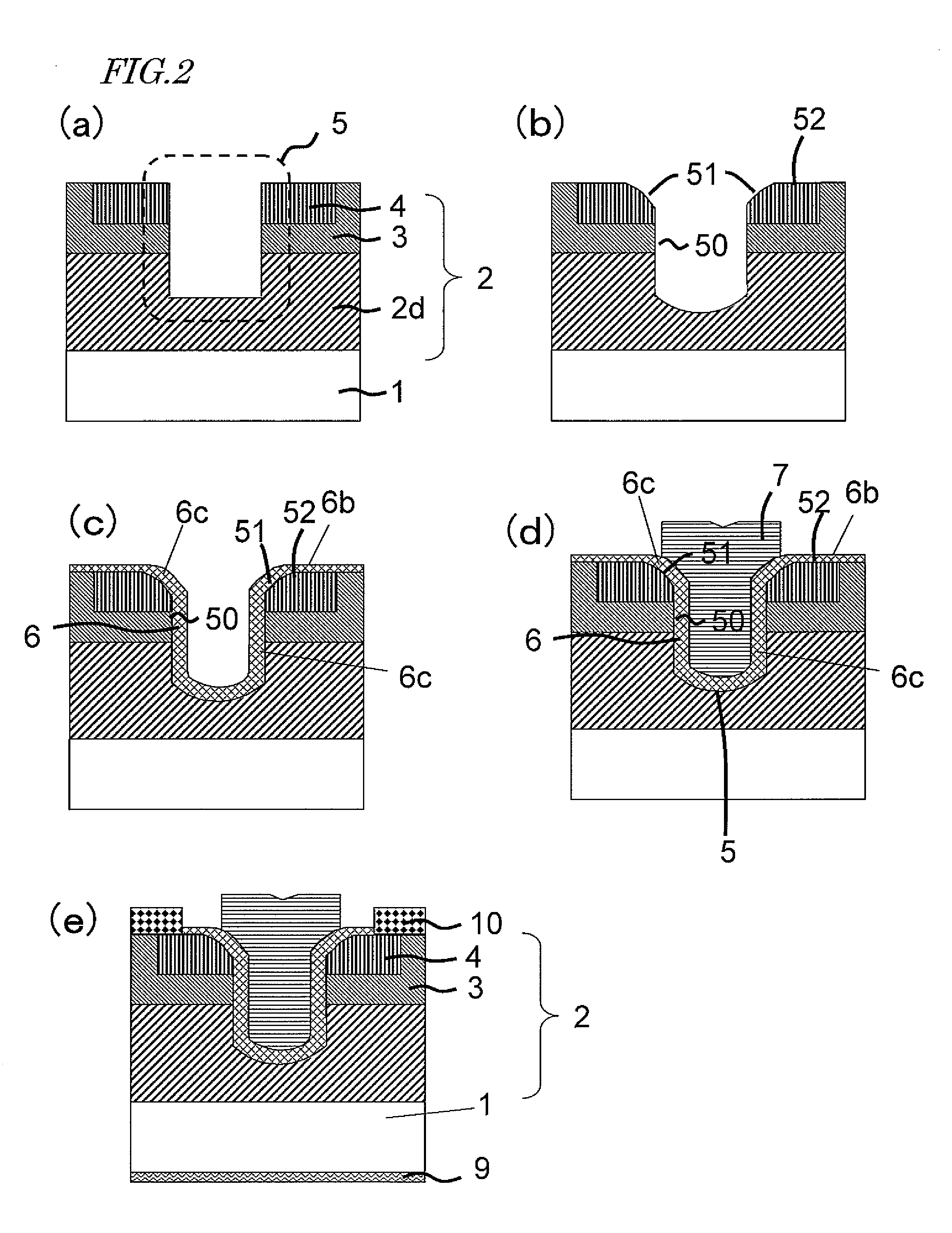
[0090]Hereinafter, a second embodiment of a silicon carbide semiconductor element according to the present invention will be described with reference to FIG. 6. FIG. 6(a) is a cross-sectional view illustrating a unit cell 200 of the silicon carbide semiconductor element of this embodiment and FIG. 6(b) is a plan view illustrating a situation where rectangular unit cells run in stripes. The unit cell 200 may also have any other shape such as a square or polygonal shape. In FIG. 6, any component also shown in FIG. 1 and having substantially the same function as its counterpart is identified by the same reference numeral and description thereof will be omitted herein for the sake of simplicity.

[0091]Each unit cell 200 of this embodiment includes a silicon carbide epitaxial layer 8 between the trench 5 and the gate insulating film 6, which is a difference from the unit cell 100 of the first embodiment shown in FIG. 1. The silicon carbide epitaxial layer 8 functions as a channel layer. I...


PUM


Abstract

A SiC semiconductor element includes: a SiC substrate which has a principal surface tilted with respect to a (0001) Si plane; a SiC layer arranged on the principal surface of the substrate; a trench arranged in the SiC layer and having a bottom, a sidewall, and an upper corner region located between the sidewall and the upper surface of the SiC layer; a gate insulating film arranged on at least a part of the sidewall and on at least a part of the upper corner region of the trench and on at least a part of the upper surface of the SiC layer; and a gate electrode arranged on the gate insulating film. The upper corner region has a different surface from the upper surface of the SiC layer and from a surface that defines the sidewall. The gate electrode contacts with both of a first portion of the gate insulating film located on the upper corner region and a second portion of the gate insulating film located on the sidewall. The first portion of the gate insulating film is thicker than a third portion of the gate insulating film located on the upper surface of the SiC layer. And an end portion of the gate electrode is located on the upper corner region.

Description

TECHNICAL FIELD[0001]The present application relates to a semiconductor element that uses SiC and a method for fabricating such an element. More particularly, the present application relates to a silicon carbide semiconductor element (as a power semiconductor device) which can be used in applications that require high breakdown voltage and a large amount of current.BACKGROUND ART[0002]Silicon carbide (SiC) has a broader band gap and a higher dielectric breakdown voltage than silicon (Si), and therefore, is expected to be the best semiconductor material to make a next-generation low-loss power device. SiC has a lot of poly-types including cubic ones such as 3C—SiC and hexagonal ones such as 6H-SIC and 4H—SiC. Among these various poly-types, the one that is used generally to make a practical silicon carbide semiconductor element is 4H—SiC.[0003]Among various power devices that use SiC, field effect transistors such as a metal-insulator-semiconductor field effect transistor (which will...

Claims


Application Information

Patent Timeline
IPC IPC(8): H01L21/02H01L29/16
CPCH01L21/0475H01L21/049H01L29/66068H01L29/872H01L21/02378H01L29/1608H01L29/8128H01L29/7827H01L29/7813
Inventor KIYOSAWA, TSUTOMUSAWADA, KAZUYUKITAKAHASHI, KUNIMASATOMITA, YUKI
Owner PANASONIC INTELLECTUAL PROPERTY MANAGEMENT CO LTD
Why Eureka
Try Eureka