Integrated circuit with a thin body field effect transistor and capacitor

a field effect transistor and integrated circuit technology, applied in the field of semiconductor devices, can solve the problems of high resistance of capacitors formed by conventional complementary metal-oxide-semiconductor (cmos) fabrication processes and thin body fets

Active Publication Date: 2013-07-11
GLOBALFOUNDRIES US INC
View PDF4 Cites 347 Cited by
  • Summary
  • Abstract
  • Description
  • Claims
  • Application Information

AI Technical Summary

Benefits of technology

[0003]One embodiment discloses an integrated circuit. The integrated circuit comprises a transistor and a capacitor. The transistor includes a first semiconductor layer and a gate stack located on the first semiconductor layer. The gate stack comprises a metal layer and a first high-k dielectric layer. A gate spacer is located on sidewalls of the gate stack. The first high-k dielectric layer is located between the first semiconductor layer and the metal layer and between the gate spacer and sidewalls of the metal layer. First and second source/drain regions are formed in a second semiconductor layer that is loca

Problems solved by technology

However, capacitors formed by conventional complementary metal-oxide-semiconductor (CMOS) fabrication pro

Method used


Image

  • Integrated circuit with a thin body field effect transistor and capacitor
  • Integrated circuit with a thin body field effect transistor and capacitor
  • Integrated circuit with a thin body field effect transistor and capacitor

Examples


Embodiment Construction

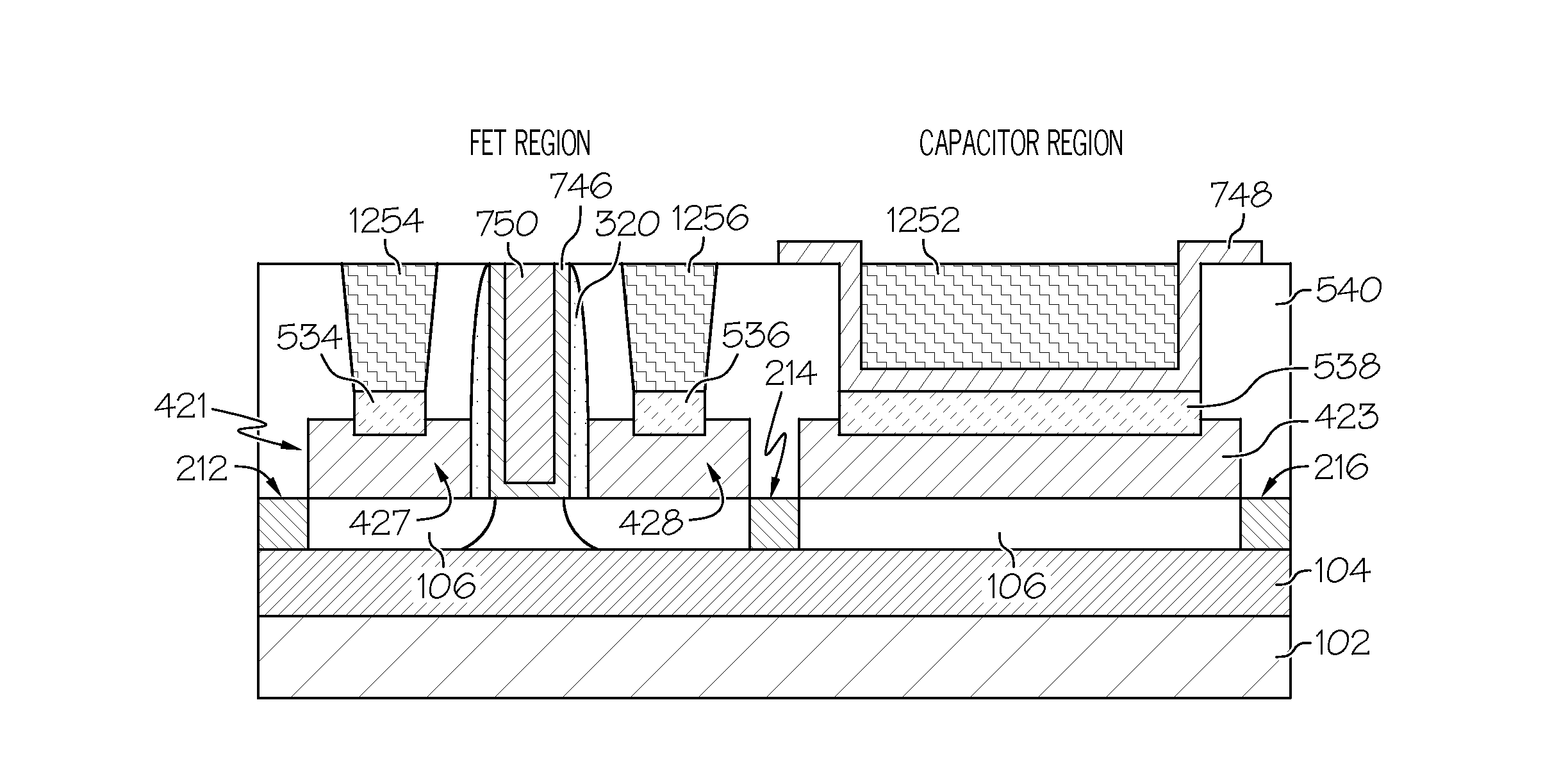
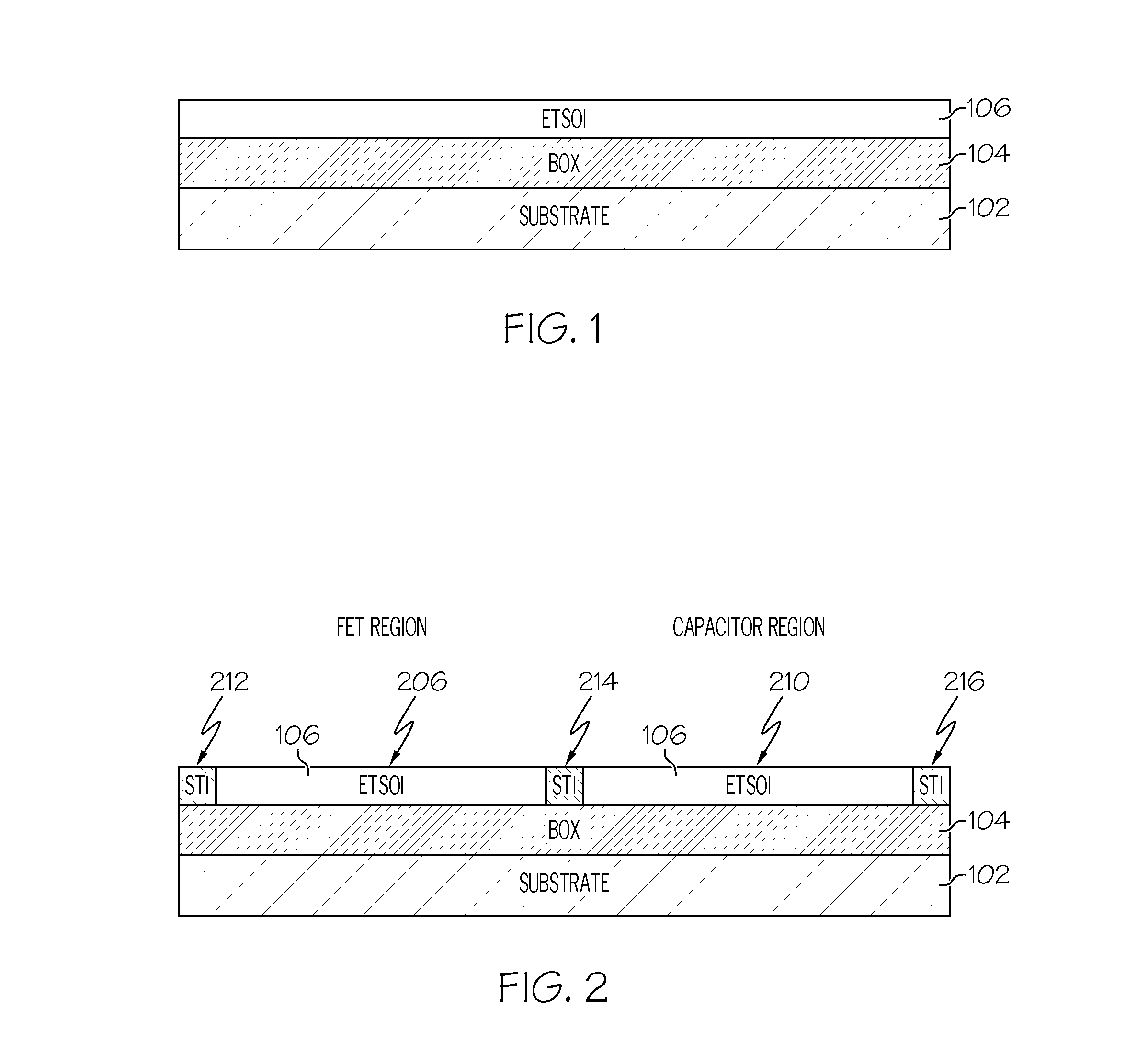
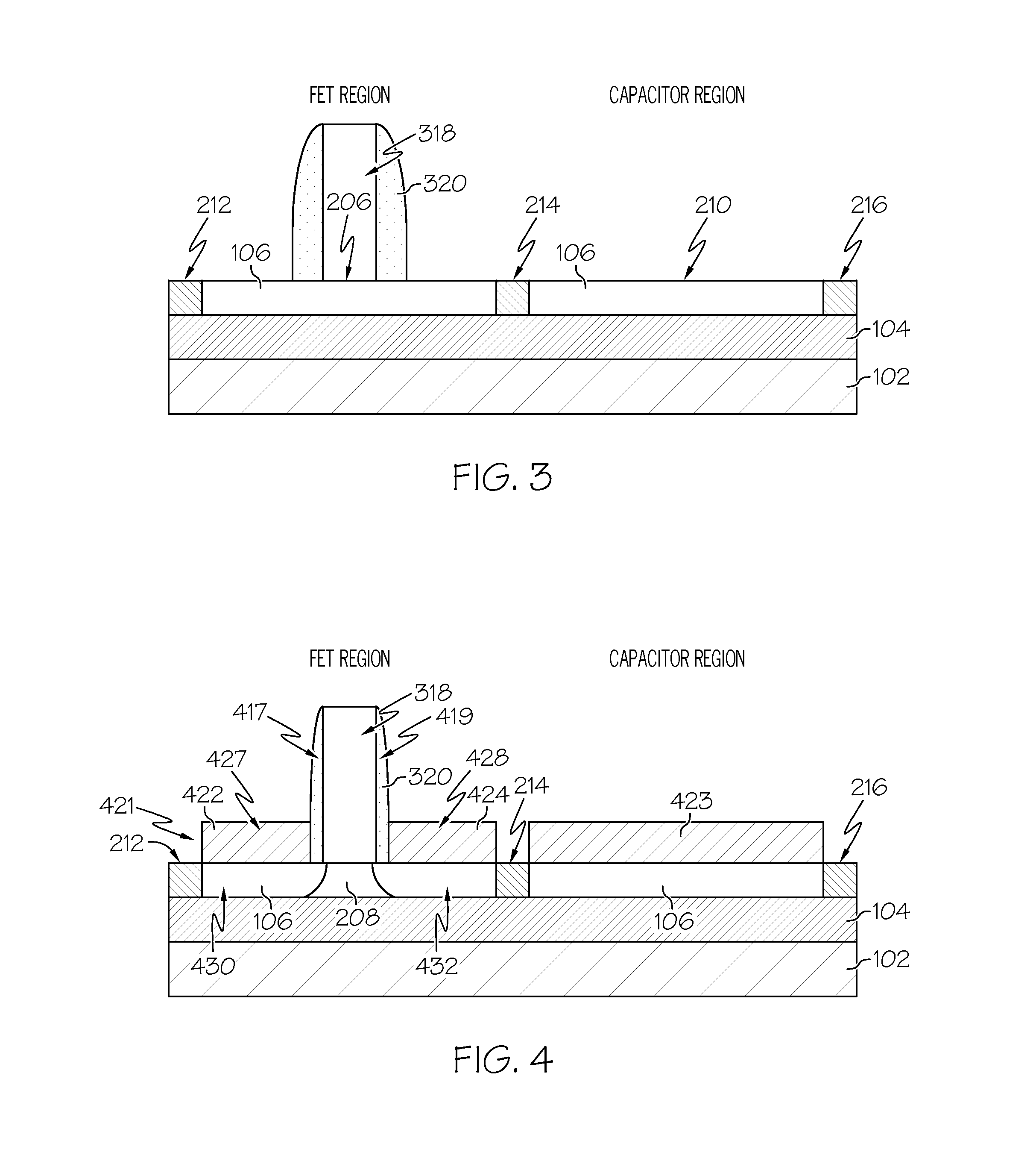
[0022]Embodiments of the present invention provide an integrated circuit that includes a fully depleted FET and an on-chip capacitor, and methods for forming such an integrated circuit. In one embodiment, an on-chip capacitor and a fully depleted FET share the same high-k dielectric and a metal layer, so as to greatly reduce process complexity and cost. Further, the capacitor has a low resistance silicide electrode and a low resistance metal electrode, so as to greatly improve the capacitor's electrical characteristics. In another embodiment, the capacitor is formed during a trench silicide / contact formation process. This allows the capacitor to have a high-k dielectric layer made of a different material than the gate dielectric of the FET, so as to achieve better electrical characteristics for the FET and the capacitor. Embodiments of the present invention are also applicable to other devices (such as finFETs and nanowire devices) in which epitaxial growth is used to form merged so...


PUM


Abstract

An integrated circuit includes a transistor and a capacitor. The transistor includes a first semiconductor layer and a gate stack located on the first semiconductor layer. The gate stack includes a metal layer and a first high-k dielectric layer. A gate spacer is located on sidewalls of the gate stack. The first high-k dielectric layer is located between the first semiconductor layer and the metal layer and between the gate spacer and sidewalls of the metal layer. A first silicide region is located on a first source/drain region. A second silicide region is located on a second source/drain region. The capacitor includes a first terminal that comprises a third silicide region located on a portion of the second semiconductor. A second high-k dielectric layer is located on the silicide region. A second terminal comprises a metal layer that is located on the second high-k dielectric layer.

Description

FIELD OF THE INVENTION[0001]The present invention generally relates to the field of semiconductors, and more particularly relates to thin body field effect transistors (FETs).BACKGROUND OF THE INVENTION[0002]Fully depleted field effect transistors (FETs) with a thin body channel, such as extremely thin silicon-on-insulator (ETSOI) and finFET devices, are now being used due to their superior device characteristics. In addition to FETs, most integrated circuits also require on-chip capacitors, such as decoupling capacitors. However, capacitors formed by conventional complementary metal-oxide-semiconductor (CMOS) fabrication processes along with thin body FETs suffer from high resistance due to the high resistance of the thin body.SUMMARY OF THE INVENTION[0003]One embodiment discloses an integrated circuit. The integrated circuit comprises a transistor and a capacitor. The transistor includes a first semiconductor layer and a gate stack located on the first semiconductor layer. The gat...

Claims


Application Information

Patent Timeline
IPC IPC(8): H01L27/06H01L21/8234
CPCH01L27/0629H01L21/84H01L27/1203H01L21/823814H01L29/41783H01L21/32053
Inventor CHENG, KANGGUODORIS, BRUCEKHAKIFIROOZ, ALISHAHIDI, GHAVAM G.
Owner GLOBALFOUNDRIES US INC
Why Eureka
Try Eureka