NEW 1T1b AND 2T2b FLASH-BASED, DATA-ORIENTED EEPROM DESIGN

a data-oriented, eeprom technology, applied in the field of new 1t1b and 2t2b flash-based, data-oriented eeprom design, can solve the problems of limiting the channel length scaling, high bit line programming voltage, and large cell size that is the largest among the nonvolatile memory structures, so as to reduce the stress on the 1t1b eeprom cell and the sl-select and bl-sel

Inactive Publication Date: 2013-07-18
APLUS FLASH TECH
View PDF6 Cites 31 Cited by
  • Summary
  • Abstract
  • Description
  • Claims
  • Application Information

AI Technical Summary

Benefits of technology

[0033]Many benefits can be achieved by applying the embodiments of the present invention. Particularly, using a novel 1T1b flash-based EEPROM cell to replace traditional 2T1b FLOTOX-based EEPROM cell remove extra source line or bit line select transistor associated with each cell so that cell size can be reduced. By introducing a novel negative control gate voltage to the word line along with a reduced bit line voltage level for bit erase operation, no need to apply high voltage to BL/SL select transistors any more. The bit line inhibit voltage is forward from a Triple P-well node voltage to the BL and SL where only a low-voltage Vdd-controlled select transistor is connected. As the result, the stress on 1T1b EEPROM cell and SL-select and BL-select HV transistors is drastically reduced and the stress-caused degradation of P/E cycles is substantially removed. The new 1T1b EEPROM cell can be further reduced in cell size as restriction from the channel length scaling limited by high BL voltage is suppressed. Therefore, the improved techniques

Problems solved by technology

Secondly, NAND Flash memory cell design uses a low-current Fowler-Nordheim tunneling phenomena for both program and erase operations.
The first disadvantage is a large cell size that is the largest among the nonvolatile memory structures.
The second disadvantage of the EEPROM memory array design is that a very high bit line programming voltage is required.
The drawback of the 2T FLOTOX-based EEPROM cell is its large cell size (for storing

Method used


Image

  • NEW 1T1b AND 2T2b FLASH-BASED, DATA-ORIENTED EEPROM DESIGN
  • NEW 1T1b AND 2T2b FLASH-BASED, DATA-ORIENTED EEPROM DESIGN
  • NEW 1T1b AND 2T2b FLASH-BASED, DATA-ORIENTED EEPROM DESIGN

Examples


Embodiment Construction

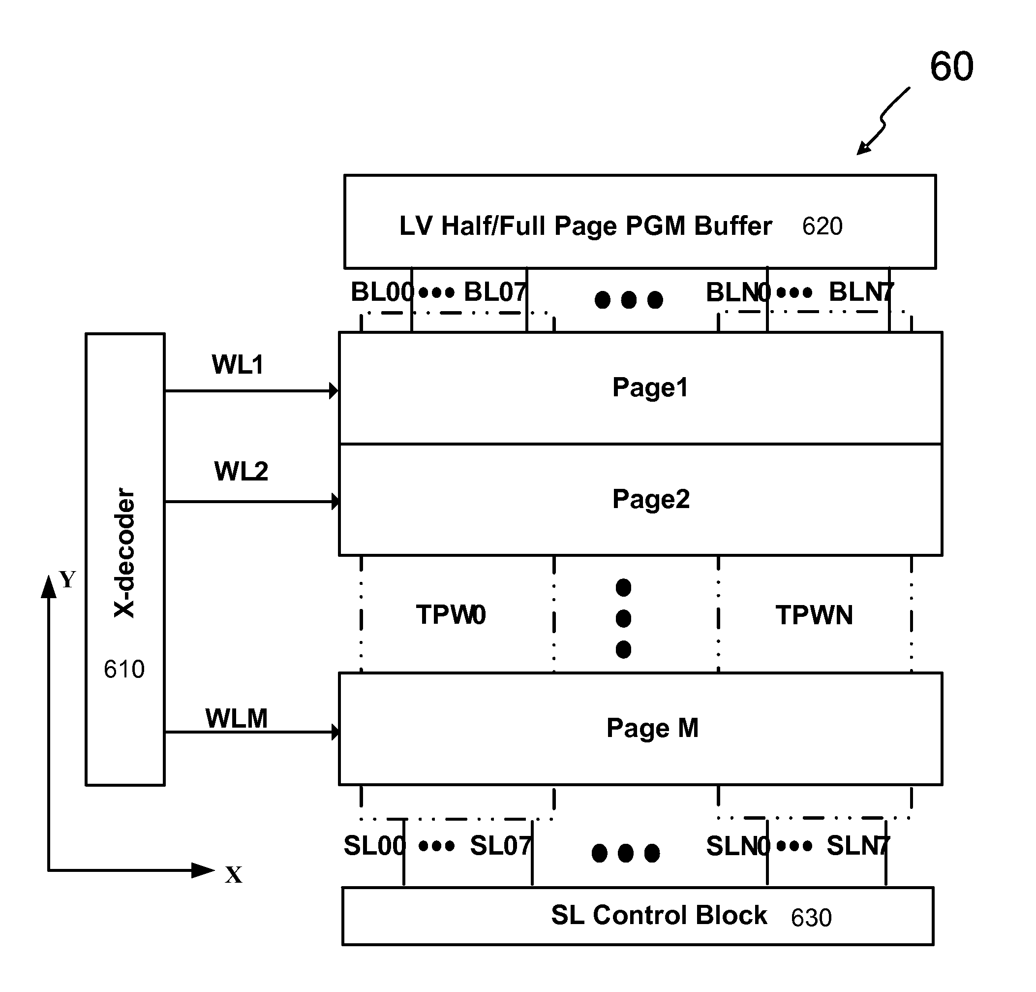
[0071]The present presentation relates to the continuation of improvement over the traditional EEPROM data-oriented Combo NVM design. But unlike an disclosure by the same inventors with the title of “A EEPROM-based, Data-oriented Combo NVM design” based on traditional large 2T1b FLOTOX-based EEPROM cell structure and process technology, the present invention provide a novel operation scheme of an 1T1b Data-oriented EEPROM cell design, which utilize a Flash-based cell structure and process made by prior art. The advantage of this single-bit 1T EEPROM cell size is about ⅓ of 90λ2 of the traditional 2T1b FLOTOX-based EEPROM cell but with a disadvantage in its operation scheme it shows of inferior of P / E endurance cycle of 300K, rather than 1M.

[0072]By contrast, when compared to the traditional NOR flash cell size, this flash-based 1T1b EEPROM cell is about 1.5× larger but its performance of the P / E endurance of 300 K is superior to the traditional NOR flash cell with 100 K cycles only....


PUM


Abstract

An one-transistor-one-bit (1T1b) Flash-based EEPROM cell is provided along with improved key operation schemes including applying a negative word line voltage and a reduced bit line voltage for perform erase operation, which drastically reduces the high voltage stress on each cell for enhancing the Program/Erase cycles while reducing cell size. An array made by the 1T1b Flash-based EEPROM cells can be operated with Half-page or Full-page divided programming and pre-charging period for each program cycle. Utilizing PGM buffer made of Vdd devices in the cell array further save silicon area. Additionally, a two-transistor-two-bit (2T2b) EEPROM cell derived from the 1T1b cell is disclosed with additional cell size reduction but with the operation of program and erase the same as that for the 1T1b cells with benefits of no process change but much enhanced storage density, superior Program/Erase endurance cycle, and capability for operating in high temperature environment.

Description

CROSS-REFERENCES TO RELATED APPLICATIONS[0001]This application claims priority to U.S. Provisional Patent Application No. 61 / 632,099, filed on Jan. 17, 2012, commonly assigned, and hereby incorporated by reference in its entirety herein for all purposes.[0002]This application is related to U.S. Pat. No. 4,599,707 and U.S. Pat. No. 6,479,347 and hereby incorporated by reference in its entirety herein for all purposes. This application is also related to U.S. patent application Ser. No. 13 / 199,785, filed on Sep. 9, 2011, U.S. patent application Ser. No. 13 / 200,010, filed on Sep. 15, 2011, and U.S. patent application Ser. No. 13 / 200,142, filed on Sep. 19, 2011, commonly assigned, and hereby incorporated by reference in its entirety herein for all purposes.BACKGROUND OF THE INVENTION[0003]The present invention relates generally to nonvolatile memory cell structure, array structure, and operation. More particularly, the present invention relates to improved 1T1b and 2T2b flash-based Elec...

Claims


Application Information

Patent Timeline
IPC IPC(8): G11C16/34G11C16/14G11C16/06
CPCG11C16/3459G11C16/06G11C16/14G11C16/0425G11C16/0483G11C16/10G11C16/16G11C16/26G11C2216/14G11C16/0458
Inventor LEE, PETER WUNGTSAO, HSING-YA
Owner APLUS FLASH TECH
Why Eureka
Try Eureka