Exposure method and exposure apparatus, and device manufacturing method

Active Publication Date: 2013-07-18
NIKON CORP
View PDF2 Cites 11 Cited by
  • Summary
  • Abstract
  • Description
  • Claims
  • Application Information

AI Technical Summary

Benefits of technology

[0019]According to this method, interference of the mask and the substrate

Problems solved by technology

However, in the conventional proximity exposure apparatus, because the gap (clearance) between the pattern surface of the mask and the surface of a photosensitive layer formed on the substrate by the photosensitive material was minimally around 30 μm, resolution was poor, therefore, the conventional proximity exposure apparatus cannot possibly be used for line widths under 64 nm which is the practical minimum line width of semiconductor devices today, such as, for example, when forming a critical pattern having a line width of 32 nm on a substrate and the like.
The liquid immersion type ArF scanner which supports the double-patterning is costly.
However, on the contrary, because the electron beam lithography has low throughput and is costly, the electron beam lithography has a disadvantage of still being far from the mass-production level.
Further, in the lithography using th

Method used


Image

  • Exposure method and exposure apparatus, and device manufacturing method
  • Exposure method and exposure apparatus, and device manufacturing method
  • Exposure method and exposure apparatus, and device manufacturing method

Examples


Embodiment Construction

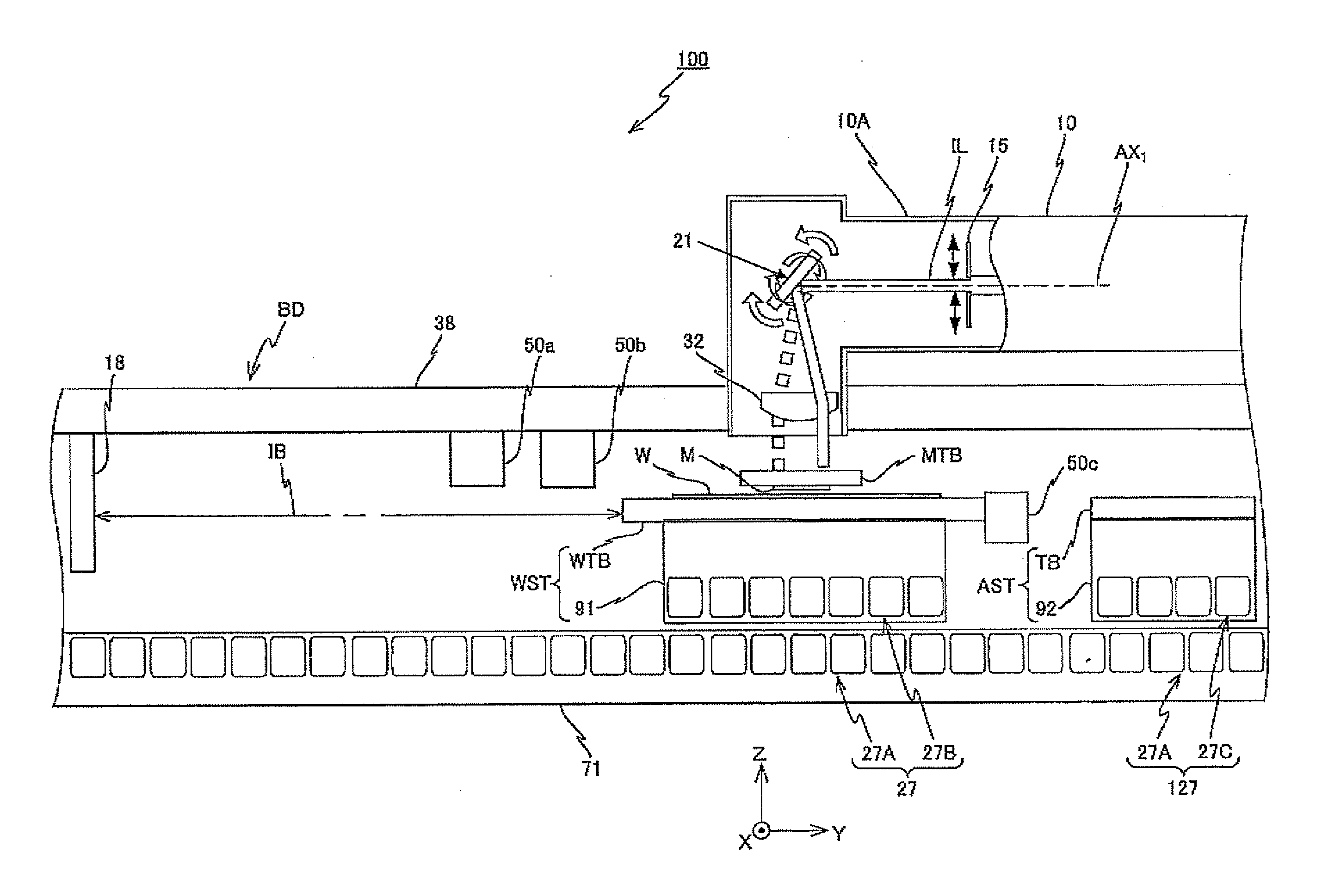
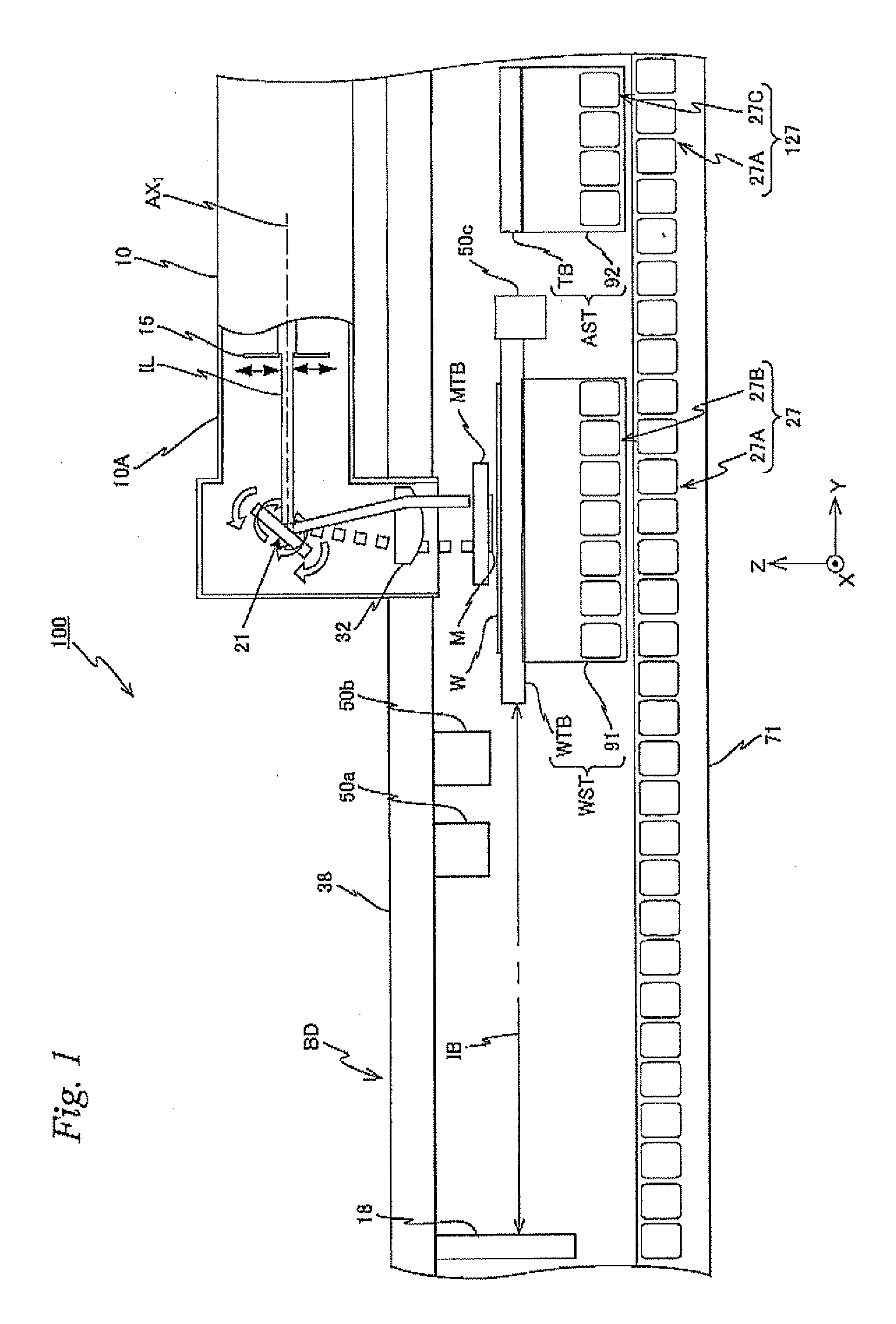
[0045]Hereinafter, an embodiment will be described, based on FIG. 1 to FIG. 21.

[0046]FIG. 1 schematically shows a structure of an exposure apparatus 100 related to the embodiment. This exposure apparatus 100 is a proximity exposure apparatus which employs a step-and-repeat method. Hereinafter, the description will be made with the lateral direction of the page surface in FIG. 1 serving as a Y-axis direction, an orthogonal direction of the page surface which is orthogonal to the Y-axis serving as an X-axis direction, and a direction orthogonal to the Y-axis and the X-axis serving as a Z-axis direction.

[0047]Exposure apparatus 100 is equipped with an illumination system 10, a mask table MTB which horizontally holds a mask M illuminated by an exposure light (illumination light) IL from the illumination system 10, a wafer stage WST which substantially holds wafer W horizontally below mask M via a predetermined gap and moves two-dimensionally parallel to a horizontal surface on a stage b...


PUM


Abstract

Exposure apparatus is equipped with an illumination optical device which illuminates a mask with an exposure beam, a mask table which holds a periphery of a pattern area of the mask from above so that a pattern surface of the mask becomes substantially parallel to an XY plane and makes a force at least parallel to an XY plane and on the mask, and a wafer stage which moves along the XY plane, holding a wafer substantially parallel to the XY plane. Therefore, an overlay with high precision of a pattern of a mask and an underlying pattern on the substrate can be realized, even though the exposure apparatus employs a proximity method, that is, the exposure apparatus does not use a projection optical system.

Description

CROSS-REFERENCE TO RELATED APPLICATIONS[0001]This application is a continuation of International Application PCT / JP2011 / 006951, with an international filing date of Dec. 13, 2011, the disclosure of which is hereby incorporated herein by reference in its entirety, which was not published in English.BACKGROUND OF THE INVENTION[0002]1. Field of the Invention[0003]The present invention relates to exposure methods and exposure apparatuses, and device manufacturing methods, and more particularly to an exposure method and an exposure apparatus by a proximity method used in a lithography process for manufacturing microdevices (electron devices) such as a semiconductor device, a liquid crystal display device and the like, and a device manufacturing method including the lithography process.[0004]2. Description of the Background Art[0005]For example, when manufacturing a semiconductor device, a liquid crystal display device, or a printed-circuit board and the like in a photolithography process...

Claims


Application Information

Patent Timeline
IPC IPC(8): G03F7/20
CPCG03F7/7035G03F7/70358G03F7/70708G03F7/70733H01L21/0273G03F7/70783G03F7/70716
Inventor SHIBAZAKI, YUICHI
Owner NIKON CORP
Why Eureka
Try Eureka