Supercharge Your Innovation With Domain-Expert AI Agents!

Semiconductor device including semiconductor memory circuit

a semiconductor memory and semiconductor technology, applied in the direction of information storage, static storage, digital storage, etc., can solve the problems of increasing the area of the mode switching circuit and difficulty in securing an adequate margin to accommodate voltage determination circuit variations, and achieve the effect of not increasing the chip area

Active Publication Date: 2013-08-01
ABLIC INC
View PDF2 Cites 0 Cited by
  • Summary
  • Abstract
  • Description
  • Claims
  • Application Information

AI Technical Summary

Benefits of technology

The present invention aims to provide a semiconductor device with a memory circuit that has a small chip area and can easily switch to a test mode without errors. The invention achieves this by configuring a mode switching circuit that can switch to a test mode without causing errors. This results in a semiconductor device that can have a smaller chip area and still perform efficient testing without any errors.

Problems solved by technology

This has been posing a problem of an increased area of the mode switching circuit.
There has been, however, a problem in that securing an adequate margin to accommodate variations in the voltage determination circuit is difficult due to deteriorated withstand voltage of a protection transistor with the increasing trend toward miniaturization of the elements in a semiconductor integrated circuit and faster element operations.

Method used


Image

  • Semiconductor device including semiconductor memory circuit
  • Semiconductor device including semiconductor memory circuit
  • Semiconductor device including semiconductor memory circuit

Examples


Embodiment Construction

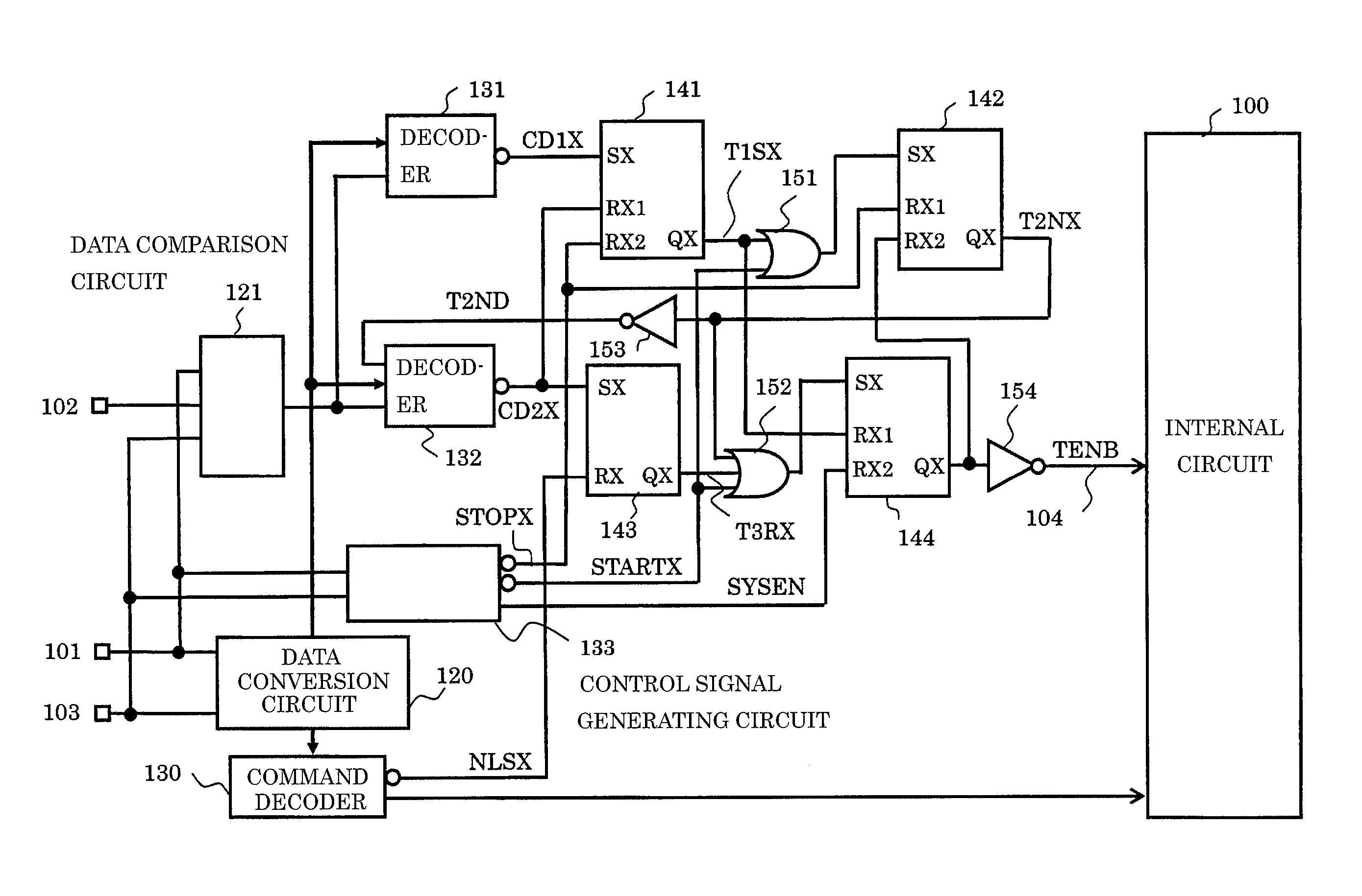
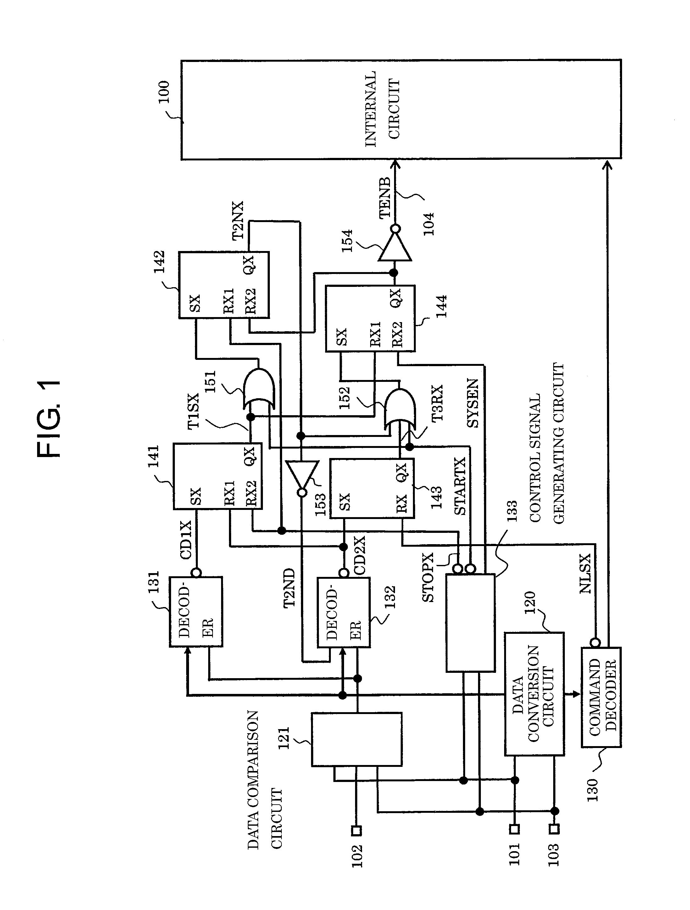
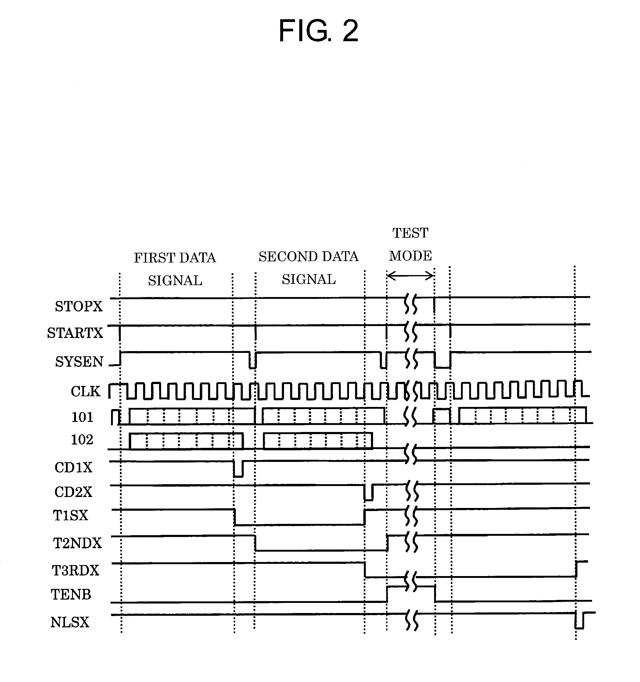
[0020]A mode switching circuit of a semiconductor device provided with a semiconductor memory circuit in accordance with the present invention has been achieved by making changes and addition to a communication circuit of the semiconductor memory circuit provided in the semiconductor device, thereby permitting mode switching to be accomplished without supplying a high voltage.

[0021]More specifically, a data comparison circuit which detects that a serial signal supplied to an input terminal for communication and a serial signal supplied to an input terminal used for a purpose other than communication are reversed from each other, a decoder circuit which detects that a serial signal carries predetermined data and which outputs a detection signal, a control signal generating circuit which generates a control signal on the basis of the serial signal, and a circuit which outputs a switching signal for switching to a test mode on the basis of the signals have been added.

[0022]The followin...


PUM


Abstract

The semiconductor device including a memory circuit is configured to include a mode switching circuit additionally provided with a data comparison circuit which detects that a serial signal supplied to an input terminal for communication and a serial signal supplied to an input terminal used for a purpose other than communication are reversed from each other, a decoder circuit which detects that a serial signal carries predetermined data and which outputs a detection signal, a control signal generating circuit which generates a control signal, and a circuit which outputs a signal for switching to a test mode on the basis of the signals.

Description

RELATED APPLICATIONS[0001]This application claims priority under 35 U.S.C. §119 to Japanese Patent Application Nos. 2012-017197 filed on Jan. 30, 2012 and 2012-245672 filed on Nov. 7, 2012, the entire contents of which are hereby incorporated by reference.BACKGROUND OF THE INVENTION[0002]1. Field of the Invention[0003]The present invention relates to a semiconductor device including a semiconductor memory circuit and, more particularly, to a mode switching circuit which permits easy switching between a normal operation mode and a test mode without an erroneous operation.[0004]2. Description of the Related Art[0005]The following describes a mode switching circuit of a semiconductor device equipped with a conventional semiconductor memory circuit. FIG. 3 is a circuit diagram illustrating a conventional mode switching circuit.[0006]The conventional mode switching circuit includes an input terminal 501, an internal circuit 502, P-type MOS transistors 503 and 504, an N-type MOS transisto...

Claims


Application Information

Patent Timeline
Patent Type & Authority Applications(United States)
IPC IPC(8): G11C8/18G11C8/10
CPCG11C8/10G11C29/46G11C8/18G11C7/10G11C7/22G11C29/00
Inventor NAKAMURA, TAKASHI
Owner ABLIC INC
Features
  • R&D
  • Intellectual Property
  • Life Sciences
  • Materials
  • Tech Scout
  • Unparalleled Data Quality
  • Higher Quality Content
  • 60% Fewer Hallucinations
Learn More