Semiconductor device

a technology of semiconductor devices and semiconductors, applied in the direction of semiconductor devices, electrical equipment, transistors, etc., can solve the problems of reducing the reliability of a semiconductor device including a transistor, and the electrical characteristics of the transistor are unstable, and achieve the effect of reliable semiconductor devices formed using transistors

Active Publication Date: 2013-08-08
SEMICON ENERGY LAB CO LTD
View PDF2 Cites 48 Cited by
  • Summary
  • Abstract
  • Description
  • Claims
  • Application Information

AI Technical Summary

Benefits of technology

[0033]According to one embodiment of the present invention, release of oxygen from side surfaces of an oxide semiconductor film including c-axis aligned crystal parts can be prevented and sufficient oxygen can be contained in the oxide semiconductor film incl...

Problems solved by technology

However, some problems of the transistor that includes an oxide semiconductor film have been pointed out.
One of the problems is unstable electrical characteristics of the transistor.
Specifically, a problem that the threshold voltage of the transistor is negatively shifted by a bias-temperature stress test (also referred to as a BT stress te...

Method used


Image

  • Semiconductor device
  • Semiconductor device
  • Semiconductor device

Examples


embodiment 1

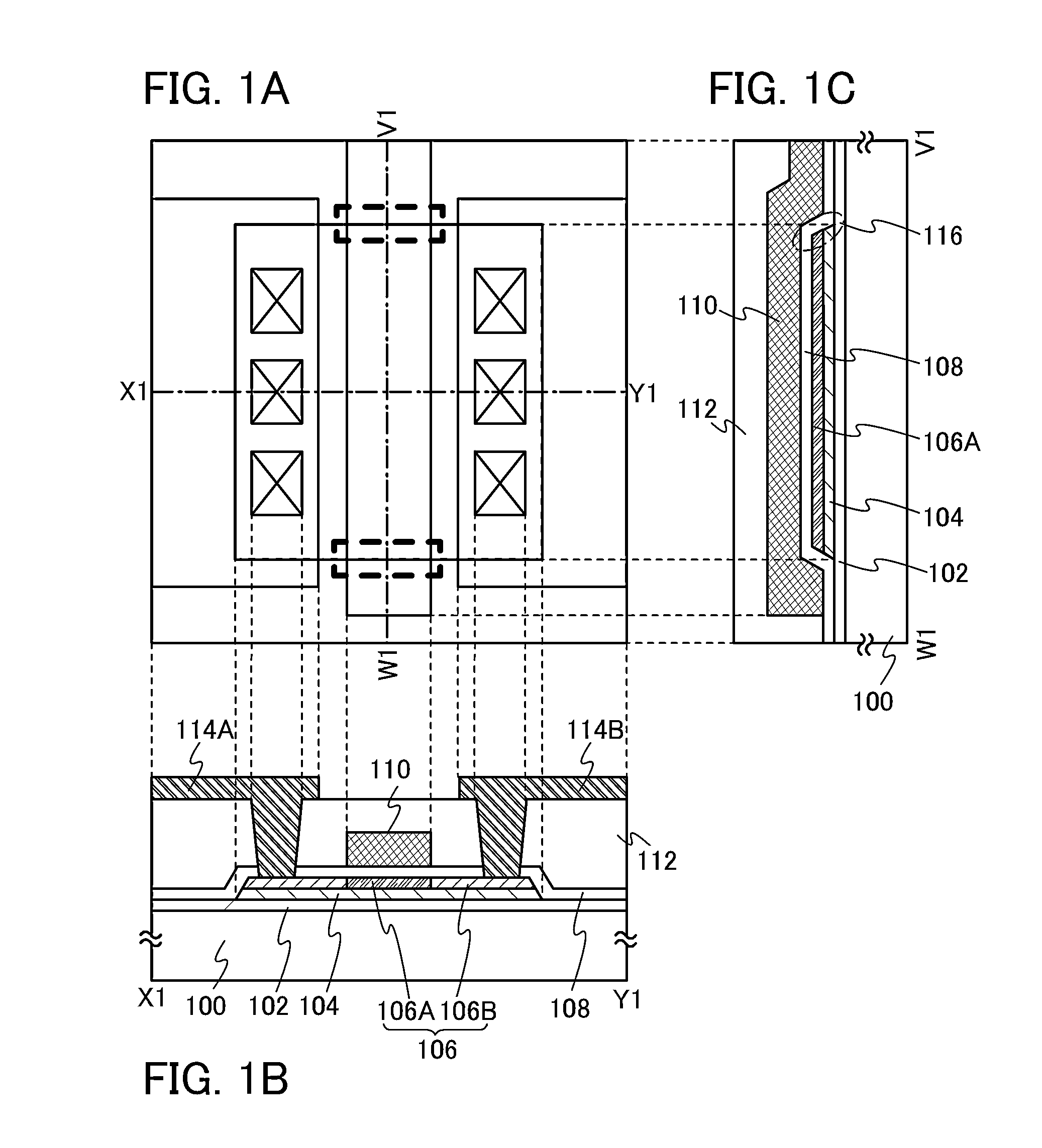
[0051]In this embodiment, a structure of a transistor that includes an oxide semiconductor film including c-axis aligned crystal parts in a semiconductor device will be described.

[0052]FIGS. 1A to 1C illustrate a transistor of one embodiment of the present invention. FIG. 1A is a plan view of the transistor. FIG. 1B is a cross-sectional view taken along line X1-Y1 in a channel length direction in FIG. 1A, and FIG. 1C is a cross-sectional view taken along line V1-W1 in a channel width direction in FIG. 1A.

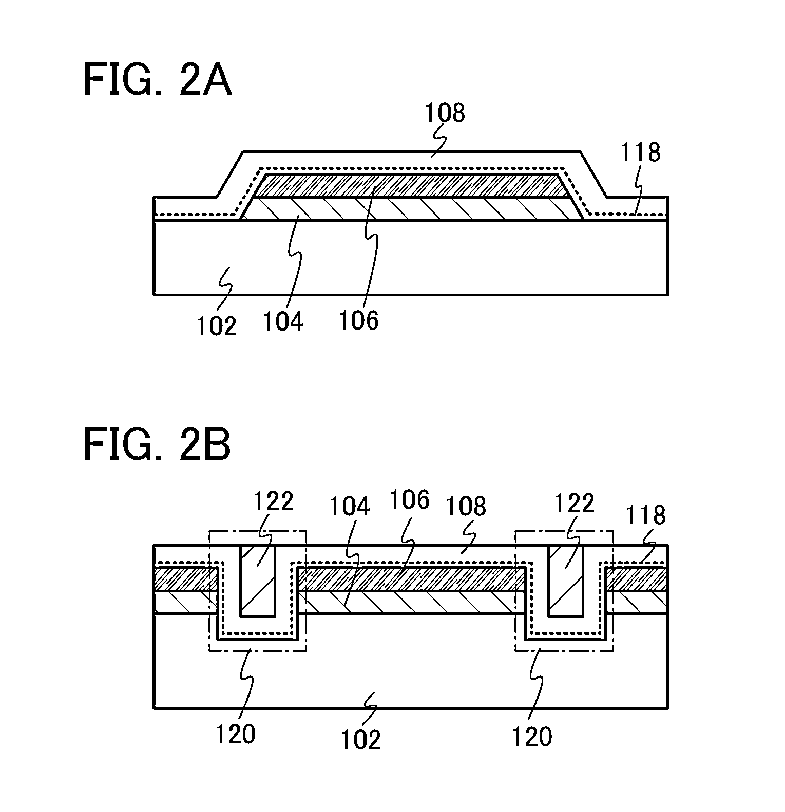
[0053]The transistor illustrated in FIGS. 1A to 1C includes an oxidation film 102 over a substrate 100, a first oxide semiconductor film 104 over the oxidation film 102, a second oxide semiconductor film 106 over the first oxide semiconductor film 104, an oxide film 108 covering at least side surfaces of the first island-like oxide semiconductor film 104 and the second island-like oxide semiconductor film 106, a gate electrode 110 over the oxide film 108, an interlayer insulating fi...

embodiment 2

[0080]In this embodiment, a structure of another transistor that includes an oxide semiconductor film including c-axis aligned crystal parts in a semiconductor device will be described together with a manufacturing method thereof, with reference to a cross-sectional view different from that used in the above embodiment.

[0081]FIGS. 3A to 3C illustrate another transistor of one embodiment of the present invention. FIG. 3A is a plan view of the transistor. FIG. 3B is a cross-sectional view taken along line X2-Y2 in a channel length direction in FIG. 3A, and FIG. 3C is a cross-sectional view taken along line V2-W2 in a channel width direction in FIG. 3A.

[0082]The transistor illustrated in FIGS. 3A to 3C includes an oxidation film 202 over a substrate 200; a first oxide semiconductor film 204 over the oxidation film 202; a second oxide semiconductor film 206 including c-axis aligned crystal parts over the first oxide semiconductor film 204; a first source electrode 214A and a first drain...

embodiment 3

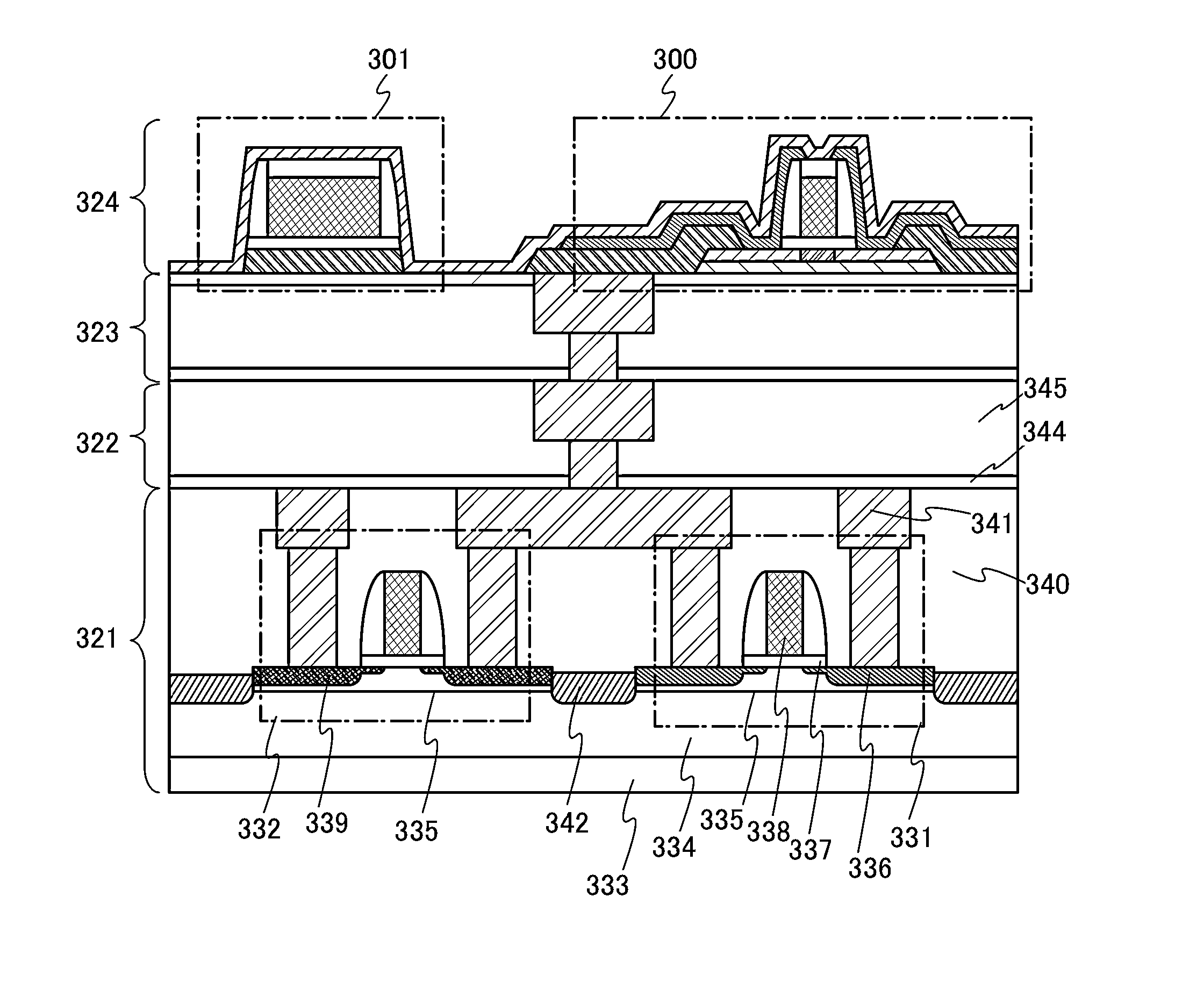
[0155]In this embodiment, the structure of the transistor described in Embodiment 2 and a capacitor that can be provided in the same layer as the transistor will be described with reference to the cross-sectional view of FIG. 7A.

[0156]A transistor 300 illustrated in the cross-sectional view of FIG. 7A corresponds to the transistor described in Embodiment 2 with reference to FIGS. 3A to 3C. The transistor 300 illustrated in FIG. 7A includes the oxidation film 202 over the substrate 200; the first oxide semiconductor film 204 over the oxidation film 202; the second oxide semiconductor film 206 over the first oxide semiconductor film 204; the first source electrode 214A and the first drain electrode 214B in contact with the side surfaces of the first island-like oxide semiconductor film 204 and the second island-like oxide semiconductor film 206 in the channel length direction; the oxide film 208 which is over part of the first island-like oxide semiconductor film 204 and the second is...


PUM


Abstract

A semiconductor device in which release of oxygen from side surfaces of an oxide semiconductor film including c-axis aligned crystal parts can be prevented is provided. The semiconductor device includes a first oxide semiconductor film, a second oxide semiconductor film including c-axis aligned crystal parts, and an oxide film including c-axis aligned crystal parts. In the semiconductor device, the first oxide semiconductor film, the second oxide semiconductor film, and the oxide film are each formed using a IGZO film, where the second oxide semiconductor film has a higher indium content than the first oxide semiconductor film, the first oxide semiconductor film has a higher indium content than the oxide film, the oxide film has a higher gallium content than the first oxide semiconductor film, and the first oxide semiconductor film has a higher gallium content than the second oxide semiconductor film.

Description

BACKGROUND OF THE INVENTION[0001]1. Field of the Invention[0002]The present invention relates to a semiconductor device including an oxide semiconductor.[0003]In this specification, a semiconductor device refers to all types of devices which can function by utilizing semiconductor characteristics; an electro-optical device, a semiconductor circuit, and an electronic device are all semiconductor devices.[0004]2. Description of the Related Art[0005]A technique by which a transistor is formed with a semiconductor thin film formed over a substrate having an insulating surface has been attracting attention. The transistor is applied to a wide range of electronic devices such as an integrated circuit (IC) and an image display device (display device). A silicon-based semiconductor material is widely known as a material for a semiconductor thin film applicable to the transistor. As another material, an oxide semiconductor has been attracting attention.[0006]For example, a transistor that in...

Claims


Application Information

Patent Timeline
IPC IPC(8): H01L29/786
CPCH01L29/7869H01L29/78693H01L29/04H01L29/78696H01L29/045H01L29/24
Inventor YAMAZAKI, SHUNPEI
Owner SEMICON ENERGY LAB CO LTD
Why Eureka
Try Eureka