Strongly correlated oxide field effect element

a field effect element and strong correlation technology, applied in the direction of basic electric elements, electrical apparatus, semiconductor devices, etc., can solve the problems of not being able to achieve colossal resistance changes (switching) such as were initially expected, and achieve the effect of reducing the thickness of the channel layer

Inactive Publication Date: 2013-08-08
FUJI ELECTRIC CO LTD
View PDF2 Cites 17 Cited by
  • Summary
  • Abstract
  • Description
  • Claims
  • Application Information

AI Technical Summary

Benefits of technology

[0040]According to any aspect of the present invention, the thickness of the channel layer can be equivalently reduced, while maintaining the metal-insulator transition

Problems solved by technology

As shown in those reports, the problem associated with field effect elements using a strongly correlated oxide as a c

Method used


Image

  • Strongly correlated oxide field effect element
  • Strongly correlated oxide field effect element
  • Strongly correlated oxide field effect element

Examples


first embodiment

1. Device Structure

1-1. Configuration Example: Structure of Field Effect Element

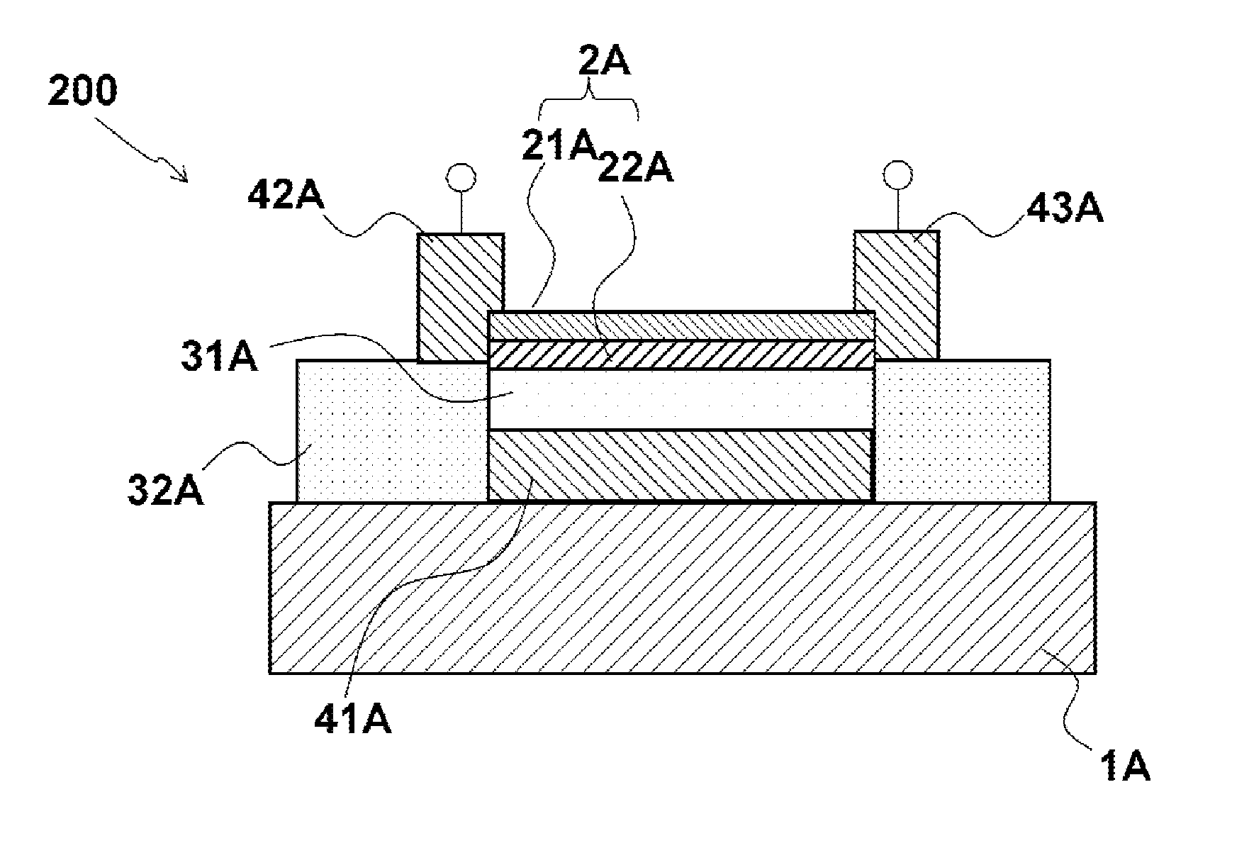
[0050]An embodiment of a field effect element using a strongly correlated oxide of the present embodiment is explained below with reference to the drawings.

[0051]FIG. 1 is a schematic sectional view illustrating the configuration of a strongly correlated oxide field effect element which is an example of the present embodiment. This figure shows the structure of a strongly correlated oxide field effect element 100 (referred to hereinbelow as “field effect element 100”) having a top-gate structure. A channel layer 2 including a metallic state layer 21 of a strongly correlated oxide and an insulator-metal transition layer 22 of a strongly correlated oxide in this order from a substrate 1 side is formed on the upper surface of the substrate 1 in FIG. 1. In the entire present application, the term “channel layer” is used merely to facilitate the understanding of the present application by comparison with a MO...


PUM


Abstract

Provided is a strongly correlated oxide field effect element demonstrating a phase transition and a switching function induced by electrical means. The strongly correlated oxide field effect element is a strongly correlated oxide field effect element 100 including a channel layer 2 constituted by a strongly correlated oxide film, a gate electrode 14, a gate insulating layer 31, a source electrode 42, and a drain electrode 43. The channel layer 2 includes an insulator-metal transition layer 22 of a strongly correlated oxide and a metallic state layer 21 of a strongly correlated oxide that are stacked on each other. The thickness t of the channel layer 2, the thickness t1 of the insulator-metal transition layer 22, and the thickness t2 of the metallic state layer 21 satisfy the following relationship with critical thicknesses t1c and t2c for respective metallic phases of the layers: t=t1+t2≧t1c>t2c, where t1<t1c and t2<t2c.

Description

TECHNICAL FIELD[0001]The present invention relates to a strongly correlated oxide field effect element. More specifically, the present invention relates to a strongly correlated oxide field effect element demonstrating a switching function induced by electrical means.BACKGROUND ART[0002]There are growing concerns that the scaling law which has been a guideline for improving performance of semiconductor devices is gradually reaching the limits. At the same time, the development of materials that will enable new operational principles necessary to get through a crisis following the transistor limit has been advanced. For example, the developments aimed at high-density nonvolatile memory devices capable of operating at a high speed equal to that of dynamic random access memory (DRAM) have been advanced in the field of spintronics incorporating the degree of freedom of electron spins.[0003]Meanwhile, the research of materials having a strongly correlated electron system to which the ban...

Claims


Application Information

Patent Timeline
IPC IPC(8): H01L29/51H01L29/78
CPCH01L29/517H01L29/78H01L49/003H01L29/78696H01L29/7869H10N99/03
Inventor OGIMOTO, YASUSHI
Owner FUJI ELECTRIC CO LTD
Why Eureka
Try Eureka