Heat treatment apparatus for heating substrate by irradiating substrate with flash of light
a technology of heat treatment apparatus and substrate, which is applied in the direction of electrical apparatus, ohmic-resistance heating, ohmic-resistance heating details, etc., can solve the problems of cracking of semiconductor wafers, high temperature of in-plane substrates, so as to improve the uniformity of in-plane temperature distribution of substrates and prevent cracking. a substrate
- Summary
- Abstract
- Description
- Claims
- Application Information
AI Technical Summary
Benefits of technology
Problems solved by technology
Method used
Image

Examples
first preferred embodiment
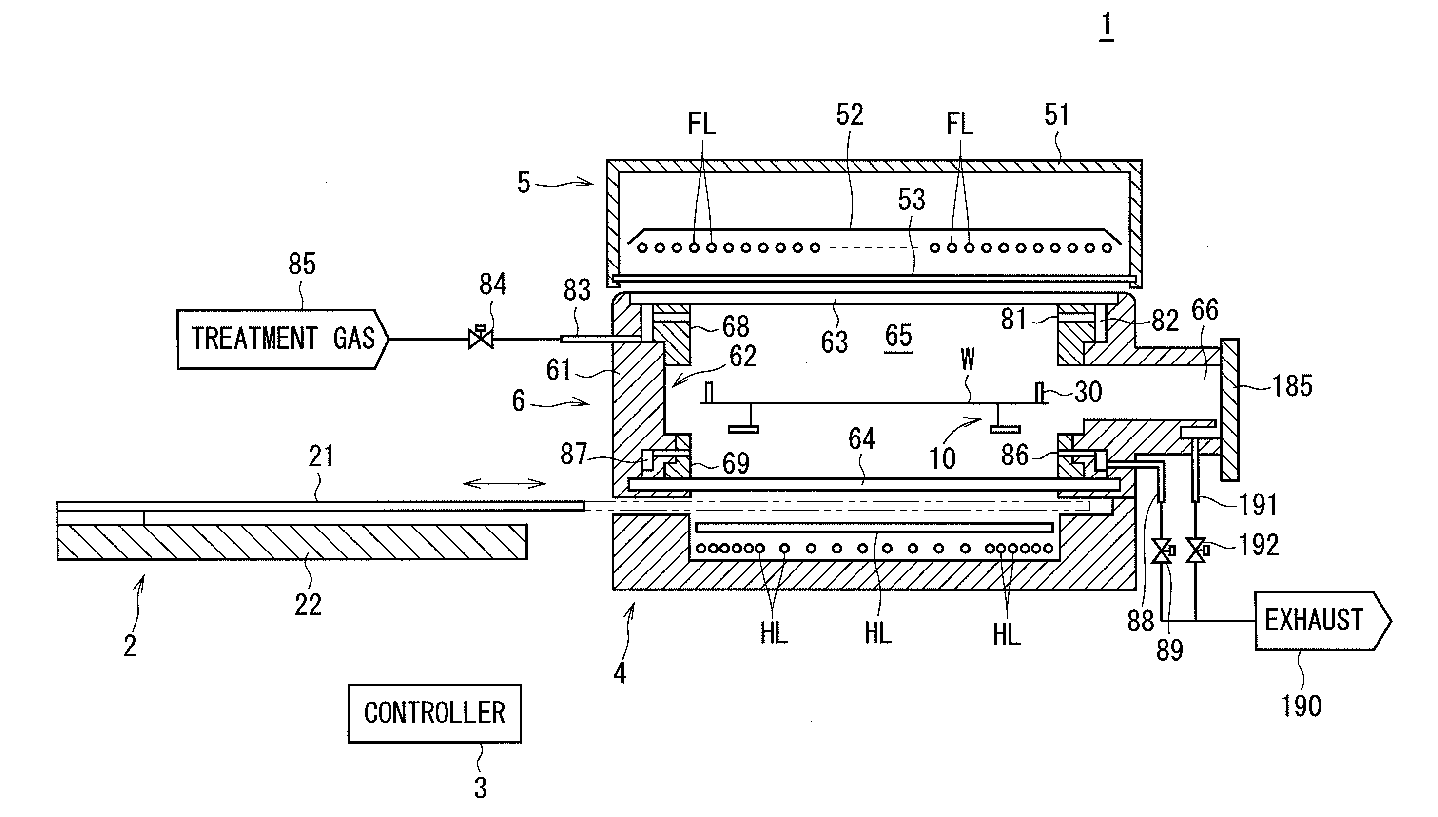
[0031]FIG. 1 is a longitudinal sectional view showing a configuration of a heat treatment apparatus 1 according to the present invention. The heat treatment apparatus 1 according to a first preferred embodiment of the present invention is a flash lamp annealer for irradiating a disk-shaped semiconductor wafer W having a diameter of 300 mm and serving as a substrate with a flash of light to heat the semiconductor wafer W. A semiconductor wafer W prior to the transport into the heat treatment apparatus 1 is implanted with impurities. The heat treatment apparatus 1 performs a heating treatment on the semiconductor wafer W to thereby activate the impurities implanted in the semiconductor wafer W. In FIG. 1 and the subsequent figures, the dimensions of components and the number of components are shown in exaggeration or in simplified form, as appropriate, for the sake of easier understanding.
[0032]The heat treatment apparatus 1 includes a chamber 6 for receiving a semiconductor wafer W t...
second preferred embodiment
[0079]Next, a second preferred embodiment according to the present invention will be described. The restriction ring 30 for abutment with the peripheral portion of a semiconductor wafer W is used in the first preferred embodiment. The second preferred embodiment differs from the first preferred embodiment in that a concave lens 130 is used in place of the restriction ring 30.
[0080]FIG. 9 is a view schematically showing the concave lens 130 in abutment with a semiconductor wafer W. The concave lens 130 according to the second preferred embodiment is provided above the support mechanism 10 (i.e., on a surface side of a semiconductor wafer W which receives a flash of light) in the chamber 6. The concave lens 130 is made of quart transparent to flashes of light from the flash lamps FL, and has a lower surface (a surface opposed to the semiconductor wafer W supported by the support mechanism 10) in the form of a concave surface 131. The concave surface 131 is a curved surface which is co...
third preferred embodiment
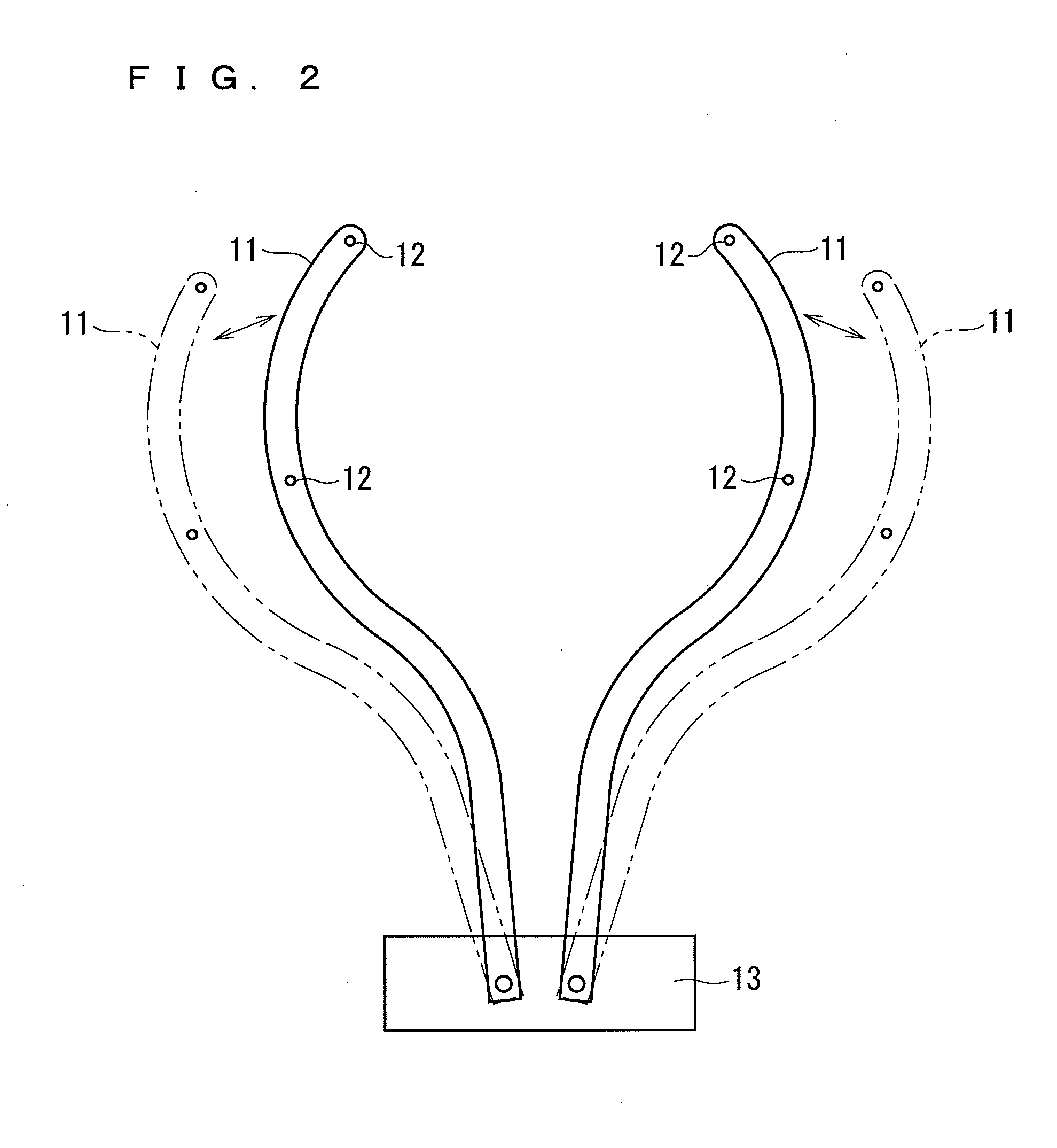
[0086]Next, a third preferred embodiment according to the present invention will be described. In the first preferred embodiment, the restriction ring 30 is in abutment with the entire perimeter of the peripheral portion WE of the semiconductor wafer W. The third preferred embodiment differs from the first preferred embodiment in that restriction blocks 230 are in abutment with only parts of the peripheral portion WE.
[0087]FIG. 10 is a view schematically showing the restriction blocks 230 in abutment with the peripheral portion WE of a semiconductor wafer W. In the third preferred embodiment, four restriction blocks 230 are provided above the support mechanism 10 (i.e., on a surface side of a semiconductor wafer W which receives a flash of light), and each of the restriction blocks 230 is brought into abutment with the peripheral portion WE. Each of the restriction blocks 230 is a rod-shaped member (a rod) made of quartz transparent to flashes of light from the flash lamps FL. The f...
PUM
 Abstract
Description
Claims
Application Information
 - R&D Engineer
- R&D Manager
- IP Professional
- Industry Leading Data Capabilities
- Powerful AI technology
- Patent DNA Extraction
Browse by: Latest US Patents, China's latest patents, Technical Efficacy Thesaurus, Application Domain, Technology Topic.
© 2024 PatSnap. All rights reserved.Legal|Privacy policy|Modern Slavery Act Transparency Statement|Sitemap