Substrate processing apparatus and substrate processing method

a substrate processing and substrate technology, applied in the direction of photosensitive materials, carpet cleaners, instruments, etc., can solve the problems of patterning shift or focal length error, short circuit, circuit malfunction, etc., and achieve the effect of greatly improving efficiency and high load

Active Publication Date: 2013-08-22
KIOXIA CORP +1
View PDF24 Cites 44 Cited by
  • Summary
  • Abstract
  • Description
  • Claims
  • Application Information

AI Technical Summary

Benefits of technology

[0009]The present invention has been made in view of the above. It is therefore an object of the present invention to provide a substrate processing apparatus and a substrate processing method which are capable of removing foreign substances from a front-side surface and / or a backside surface of a substrate, such as a wafer, at high removal efficiency. More particularly, it is an object of the present invention to provide a substrate processing apparatus and a substrate processing method which are capable of cleaning and drying the substrate after removing the foreign substances from the substrate.
[0012]According to embodiments of the present invention, the second surface of the substrate (e.g., a front-side surface of the substrate) is supported by the hydrostatic support mechanism. Therefore, the scrubber can apply a relatively high load to the first surface of the substrate (e.g., a backside surface of the substrate). Under such a high load, the scrubbing member of the scrubber is placed in sliding contact with the first surface to thereby slightly scrape off the first surface. Consequently, the scrubber can remove the foreign substances firmly attached to the first surface. In particular, the scrubber can remove the foreign substances having a size of 100 nm or more with greatly improved efficiency. Moreover, since the second surface of the substrate is supported by the hydrostatic support mechanism which does not contact the substrate, the scrubber can remove the foreign substances from the first surface without causing damage to devices formed on the second surface.
[0013]Furthermore, according to embodiments of the present invention, the substrate processing apparatus can remove the foreign substances from the substrate, clean the substrate, and dry the substrate. Therefore, it is not necessary to transport the substrate to other sites for these processes. That is, the substrate can be scrubbed, cleaned, and dried successively in one processing chamber, so that debris and mists (e.g., processing liquid and cleaning liquid) are prevented from spreading out. As a consequence, the substrate processing apparatus can be installed in a clean environment, such as a clean room.

Problems solved by technology

The foreign substances attached to the devices could be a cause of a short circuit between interconnects and a malfunction of the circuit.
The foreign substances on the backside surface of the wafer may cause the wafer to be separated from a stage reference surface of an exposure apparatus and / or may cause the wafer surface to tilt with respect to the stage reference surface, resulting in a patterning shift or a focal length error.
However, such a cleaning technique has a low capability of removing the foreign substances.
In particular, it is difficult for the conventional cleaning technique to remove the foreign substances having a size of 100 nm or more.

Method used


Image

  • Substrate processing apparatus and substrate processing method
  • Substrate processing apparatus and substrate processing method
  • Substrate processing apparatus and substrate processing method

Examples


example 1

(1) Example 1

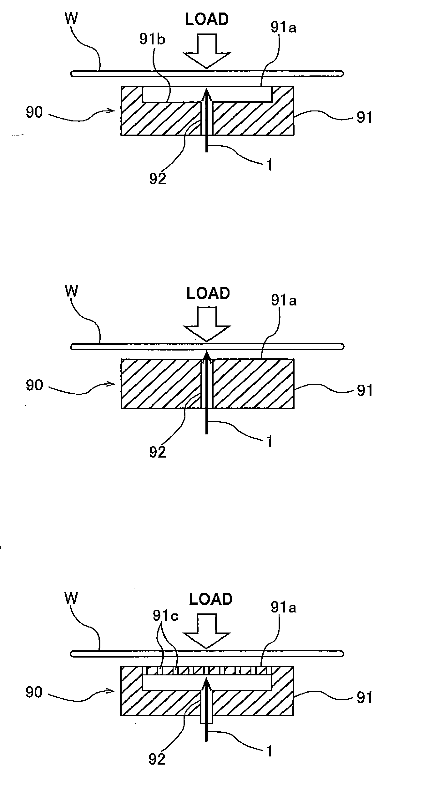
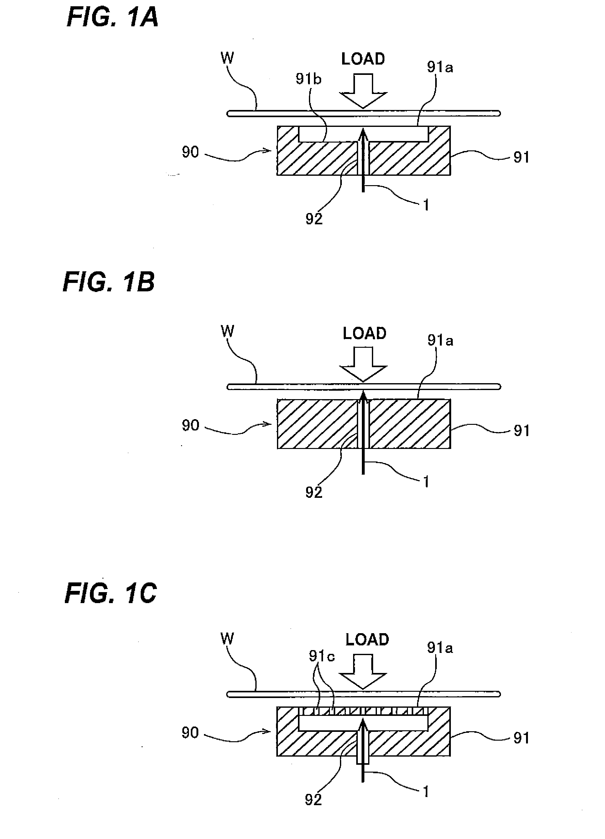
[0066]More specific examples of the substrate processing apparatus including the hydrostatic support mechanism 90 will be described below with reference to FIGS. 3A and 3B. FIG. 3A is a conceptual view of the substrate processing apparatus including the hydrostatic support mechanism 90 disposed below the substrate W. The hydrostatic support mechanism 90 has the fluid supply passage 92 for the pressure fluid 1. The pressure fluid 1 is supplied to the fluid supply passage 92 through a supply pipe (not shown). Before processing of the substrate W is started, the support stage 91 of the hydrostatic support mechanism 90 is elevated toward the substrate W. After the substrate W is processed, the support stage 91 is lowered. Alternatively, the substrate processing apparatus may have a mechanism for elevating and lowering the substrate W. In FIG. 3A, the hydrostatic support mechanism 90 has the structure shown in FIG. 1A. The hydrostatic support mechanism 90 may have the struct...

example 2

(2) Example 2

[0071]FIG. 3B is a conceptual view of the substrate processing apparatus including the hydrostatic support mechanism 90 disposed above the substrate W. The substrate processing apparatus shown in FIG. 3B has basic structures identical to those of the substrate processing apparatus shown in FIG. 3A.

example 3

(3) Example 3

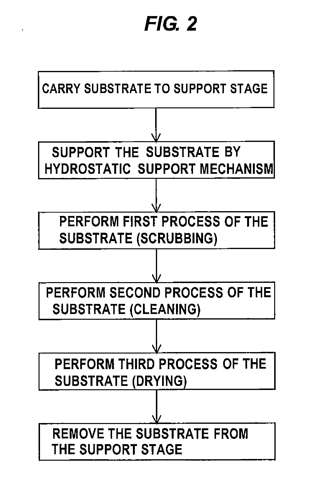
[0072]A method of performing surface processing of the substrate using the substrate processing apparatus according to an embodiment of the present invention will be described below. A substrate (e.g., a substrate in the process of LSI fabrication) is placed in the substrate processing apparatus with its one-side surface (e.g., a device surface) facing the hydrostatic support mechanism 90 and the opposite surface (e.g., the backside surface) facing the processing head 50. The peripheral edge of the substrate is held by the chucks 11. The substrate is then rotated while its device surface is supported by the hydrostatic support mechanism 90. In this state, the processing head 50 presses the backside surface, on which no device is formed, of the substrate to remove scratches and particles from the backside surface. The substrate may not be held by the chucks 11 throughout the surface processing.

[0073]When scrubbing of the substrate is performed, the backside surface of th...


PUM


Abstract

A substrate processing apparatus removes foreign substances from a substrate at high removal efficiency. The substrate processing apparatus includes: a scrubber to perform surface processing of the substrate by bringing a scrubbing member into sliding contact with a first surface of the substrate, a hydrostatic support mechanism for supporting a second surface of the substrate via fluid pressure without contacting the substrate, the second surface being an opposite surface of the first surface, a cleaner to clean the processed substrate, and a dryer to dry the cleaned substrate. The scrubber brings the scrubbing member into sliding contact with the first surface while rotating the scrubbing member about a central axis of the scrubber.

Description

CROSS REFERENCE TO RELATED APPLICATIONS[0001]This document claims priority to Japanese Patent Application No. 2012-35365, filed on Feb. 21, 2012, the entire contents of which are hereby incorporated by reference.BACKGROUND OF THE INVENTION[0002]1. Field of the Invention[0003]The present invention relates to an apparatus and a method for processing a front-side surface and / or a backside surface of a substrate, such as a wafer, which requires high cleanliness.[0004]2. Description of the Related Art[0005]In recent years, various devices including memory circuits, logic circuits, and image sensors (e.g., complimentary metal-oxide-semiconductor (CMOS) sensors) have become more and more highly integrated. In the processes of fabricating these devices, foreign substances, such as fine particles and dusts, may be attached to the devices. The foreign substances attached to the devices could be a cause of a short circuit between interconnects and a malfunction of the circuit. Therefore, in or...

Claims


Application Information

Patent Timeline
Patent Type & Authority Applications(United States)
IPC IPC(8): B08B1/00
CPCB08B1/001H01L21/67046H01L21/68728H01L21/67051H01L21/67132H01L21/68764
Inventor ISHII, YUKAWASAKI, HIROYUKINAGAOKA, KENICHIITO, KENYAKODERA, MASAKOTOMITA, HIROSHINISHIOKA, TAKESHI
Owner KIOXIA CORP
Why Eureka
Try Eureka