Method for filling trench with metal layer and semiconductor structure formed by using the same

Active Publication Date: 2013-08-22
UNITED MICROELECTRONICS CORP
View PDF25 Cites 14 Cited by
  • Summary
  • Abstract
  • Description
  • Claims
  • Application Information

AI Technical Summary

Benefits of technology

[0009]The present invention provides a method including at least two deposition processes to fill the trench with the metal lay

Problems solved by technology

With the development of technology and the increasingly imaginative applications of electrical products, IC devices are becoming smaller, more delicate and more diversified.
Along with the miniaturization of the IC device, however, manufacturers have encountered problems related to IC fabrication methods.
Due to the shrinkage of the device size as a consequence of dev

Method used


Image

  • Method for filling trench with metal layer and semiconductor structure formed by using the same
  • Method for filling trench with metal layer and semiconductor structure formed by using the same
  • Method for filling trench with metal layer and semiconductor structure formed by using the same

Examples


Example

[0014]To provide a better understanding of the present invention, preferred embodiments will be described in detail. The preferred embodiments of the present invention are illustrated in the accompanying drawings with numbered elements.

[0015]The present invention provides a method for filling a trench with a metal layer, in which at least two deposition processes are performed. By adjusting the temperature, the supplement of heat transferring gas, and the power supply during the deposition, the metal layer can obtain a better gap filling ability.

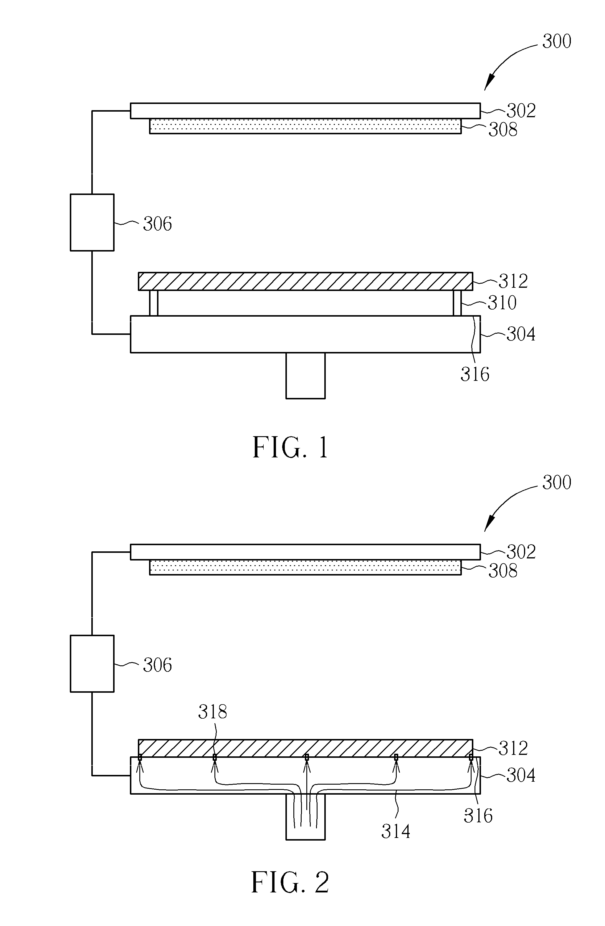
[0016]Please refer to FIG. 1 and FIG. 2, which illustrate schematic diagrams of the deposition apparatus according to the present invention. As shown in FIG. 1, the deposition apparatus 300 in the present invention includes a cathode 302 and an anode 304, which are connected to a bias voltage unit 306. The bas voltage unit 306 is able to provide sufficient voltage for the cathode 302 and the anode 304 during the deposition process. A target ...


PUM


Abstract

A method for filling a trench with a metal layer is disclosed. A deposition apparatus having a plurality of supporting pins is provided. A substrate and a dielectric layer disposed thereon are provided. The dielectric layer has a trench. A first deposition process is performed immediately after the substrate is placed on the supporting pins to form a metal layer in the trench, wherein during the first deposition process a temperature of the substrate is gradually increased to reach a predetermined temperature. When the temperature of the substrate reaches the predetermined temperature, a second deposition process is performed to completely fill the trench with the metal layer.

Description

BACKGROUND OF THE INVENTION[0001]1. Field of the Invention[0002]The present invention relates to a method for filling a trench with a metal layer and a semiconductor structure formed by using the same, and more particularly, to a method including at least two deposition processes for filling a trench with a metal layer and a semiconductor structure formed by using the same.[0003]2. Description of the Prior Art[0004]Micro-processor systems comprised of integrated circuits (IC) are ubiquitous devices in modern society, being utilized in such diverse fields as automatic control electronics, mobile communication devices and personal computers. With the development of technology and the increasingly imaginative applications of electrical products, IC devices are becoming smaller, more delicate and more diversified.[0005]Along with the miniaturization of the IC device, however, manufacturers have encountered problems related to IC fabrication methods. For example, aluminum is material com...

Claims


Application Information

Patent Timeline
IPC IPC(8): H01L29/78H01L29/45H01L21/768
CPCH01L21/2855H01L21/76877H01L21/28079H01L21/28088H01L29/513H01L23/53223H01L29/518H01L29/66545H01L21/76846H01L21/76879H01L23/5226H01L29/517H01L2924/0002H01L2924/00
Inventor HSU, CHI-MAOHUANG, HSIN-FUTSAI, MIN-CHUANCHEN, CHIEN-HAOCHEN, WEI-YULIN, CHIN-FULI, JING-GANGCHEN, MIN-HSIENSU, JIAN-HONG
Owner UNITED MICROELECTRONICS CORP
Why Eureka
Try Eureka